STM8S903K3 STM8S903F3
Conversion time: 14 clock cycles
Product overview
•
•
•
•
•
•
•
•
•
•
Single and continuous and buffered continuous conversion modes
Buffer size (n x 10 bits) where n = number of input channels
Scan mode for single and continuous conversion of a sequence of channels
Analog watchdog capability with programmable upper and lower thresholds
Internal reference voltage on channel AIN7
Analog watchdog interrupt
External trigger input
Trigger from TIM1 TRGO
End of conversion (EOC) interrupt
Internal bandgap reference voltage
Channel AIN7 is internally connected to the internal bandgap reference voltage. The internal
bandgap reference is constant and can be used, for example, to monitor VDD. It is independent
of variations in VDD and ambient temperature TA.
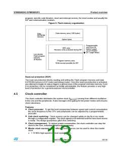
4.14
Communication interfaces
The following communication interfaces are implemented:
UART1: Full feature UART, synchronous mode, SPI master mode, Smartcard mode, IrDA
mode, single wire mode, LIN2.1 master capability
•
SPI : Full and half-duplex, 8 Mbit/s
•
I²C: Up to 400 Kbit/s
•
4.14.1
UART1
Main features
One Mbit/s full duplex SCI
•
SPI emulation
•
High precision baud rate generator
•
Smartcard emulation
•
IrDA SIR encoder decoder
•
LIN master mode
•
Single wire half duplex mode
•
Asynchronous communication (UART mode)
Full duplex communication - NRZ standard format (mark/space)
•
Programmable transmit and receive baud rates up to 1 Mbit/s (fCPU/16) and capable of
following any standard baud rate regardless of the input frequency
•
Separate enable bits for transmitter and receiver
•
Two receiver wakeup modes:
•
Address bit (MSB)
-
Idle line (interrupt)
-
DocID15590 Rev 8
17/116

 STMICROELECTRONICS [ ST ]