STM32F105xx, STM32F107xx
Applicative block diagrams
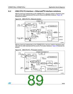
A.4
USB OTG FS interface + Ethernet/I2S interface solutions
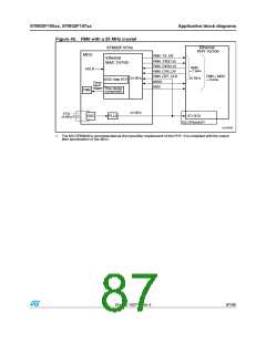
With the clock tree implemented on the STM32F107xx, only one crystal is required to work
with both the USB (host/device/OTG) and the Ethernet (MII/RMII) interfaces. Figure 48
illustrate the solution.
Figure 48. USB OTG FS + Ethernet solution
STM32F107
MCU
Div
by 5
XTAL
PLL2
x8
25 MHz
Cortex-M3 core
up to
72 MHz
PLL
x9
VCO
Out
x18
Div
by 5
OTG
48 MHz
PHY
Div by 3
sel
PLL3 Up to
50 MHz
MCLK
SCLK
x10
2% accuracy
error
I2S
MCO
Ethernet
PHY
MCO
sel
ai15662b
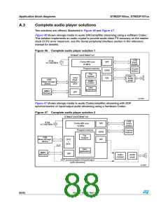
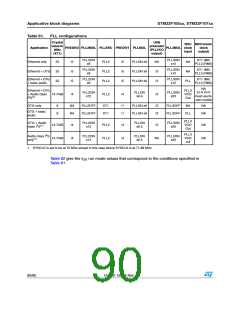
With the clock tree implemented on the STM32F107xx, only one crystal is required to work
2
with both the USB (host/device/OTG) and the I S (Audio) interfaces. Figure 49 illustrate the
solution.
2
Figure 49. USB OTG FS + I S (Audio) solution
STM32F105/STM32F107
XTAL
MCU
14.7456 MHz
Div
by 4
PLL2
x12
Cortex-M3 core
Up to
71.88 MHz
PLL
x6.5
VCO
Out
Div
by 4
OTG
47.9232 MHz
PHY
Div by 3
x13
sel
PLL3
0.16% accuracy error
VCO
Out
x40
MCLK
MCO
Less than 0.5% accuracy
error on MCLK and SCLK
I2S
MCO
Up to
147.456 MHz
SCLK
ai15663b
Doc ID 15274 Rev 4
89/95

 STMICROELECTRONICS [ ST ]