Applicative block diagrams
STM32F105xx, STM32F107xx
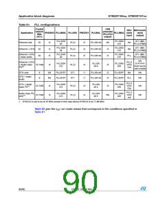
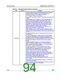
Table 61. PLL configurations
Crystal
value in
MHz
USB
I2Sn MCO (main
prescaler
(PLLVCO
output)
Application
PREDIV2 PLL2MUL PLLSRC PREDIV1 PLLMUL
PLL3MUL clock
clock
input
output)
(XT1)
PLL2ON
x8
PLL3ON
x10
XT1 (MII)
PLL3 (RMII)
Ethernet only
25
25
25
/5
/5
/5
PLL2
PLL2
PLL2
/5
/5
/5
PLLON x9
PLLON x9
PLLON x9
NA
/3
NA
NA
PLL2ON
x8
PLL3ON
x10
XT1 (MII)
PLL3 (RMII)
Ethernet + OTG
Ethernet + OTG
+ basic audio
PLL2ON
x8
PLL3ON
x10
XT1 (MII)
PLL3 (RMII)
/3
PLL
NA
Ethernet + OTG
+ Audio class
I2S(1)
PLL3
VCO
Out
PLL2ON
x12
PLLON
x6.5
PLL3ON
x20
ETH PHY
must use its
own crystal
14.7456
/4
PLL2
/4
/3
OTG only
8
8
NA
NA
PLL2OFF
PLL2OFF
XT1
XT1
/1
/1
PLLON x9
PLLON x9
/3
/3
PLL3OFF
NA
NA
NA
OTG + basic
audio
PLL3OFF PLL
PLL3
OTG + Audio
class I2S(1)
PLL2ON
x12
PLLON
x6.5
PLL3ON
VCO
x20
14.7456
14.7456
/4
/4
PLL2
PLL2
/4
/4
/3
NA
NA
Out
PLL3
Audio class I2S
only(1)
PLL2ON
x12
PLLON
x6.5
PLL3ON
VCO
x20
NA
out
1. SYSCLK is set to be at 72 MHz except in this case where SYSCLK is at 71.88 MHz.
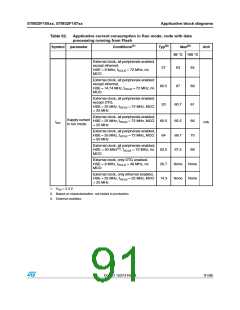
Table 62 give the I run mode values that correspond to the conditions specified in
DD
Table 61.
90/95
Doc ID 15274 Rev 4

 STMICROELECTRONICS [ ST ]