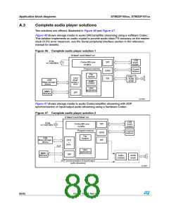
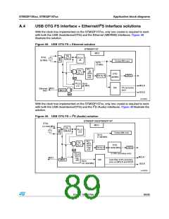
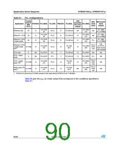
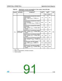
PDF
最近搜索
热门搜索
发布采购

| 型号: | STM32F105RBT6 |
| PDF下载: | 下载PDF文件 查看货源 |
| 内容描述: | [Mainstream Connectivity line, ARM Cortex-M3 MCU with 128 Kbytes Flash, 72 MHz CPU, CAN, USB 2.0 OTG] |
| 分类和应用: | 以太网通信 |
| 文件页数/大小: | 95 页 / 1009 K |
| 品牌: |  STMICROELECTRONICS [ ST ] STMICROELECTRONICS [ ST ] |
专业IC领域供求交易平台:提供全面的IC Datasheet资料和资讯,Datasheet 1000万数据,IC品牌1000多家。