Electrical characteristics
STM32F405xx, STM32F407xx
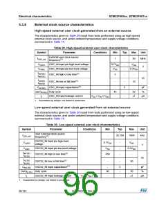
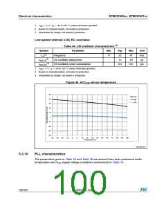
5.3.8
External clock source characteristics
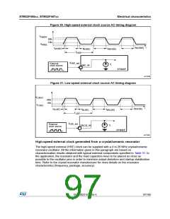
High-speed external user clock generated from an external source
The characteristics given in Table 29 result from tests performed using an high-speed
external clock source, and under ambient temperature and supply voltage conditions
summarized in Table 14.
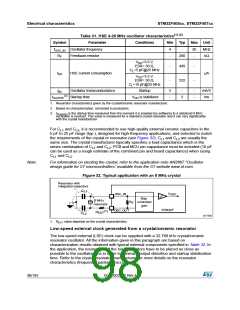
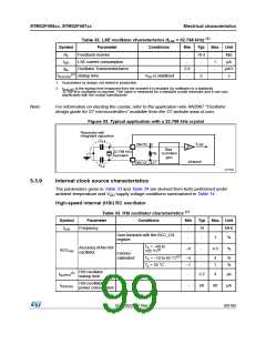
Table 29. High-speed external user clock characteristics
Symbol
Parameter
Conditions
Min
Typ
Max
Unit
External user clock source
frequency(1)
fHSE_ext
1
-
50
MHz
VHSEH
VHSEL
tw(HSE)
OSC_IN input pin high level voltage
OSC_IN input pin low level voltage
0.7VDD
VSS
-
-
VDD
V
0.3VDD
OSC_IN high or low time(1)
OSC_IN rise or fall time(1)
5
-
-
-
-
tw(HSE)
ns
tr(HSE)
tf(HSE)
10
Cin(HSE) OSC_IN input capacitance(1)
-
45
-
5
-
-
pF
%
DuCy(HSE) Duty cycle
55
±1
IL
OSC_IN Input leakage current
VSS ≤ VIN ≤ VDD
-
µA
1. Guaranteed by design, not tested in production.
Low-speed external user clock generated from an external source
The characteristics given in Table 30 result from tests performed using an low-speed
external clock source, and under ambient temperature and supply voltage conditions
summarized in Table 14.
Table 30. Low-speed external user clock characteristics
Symbol
Parameter
Conditions
Min
Typ
Max
Unit
User External clock source
frequency(1)
fLSE_ext
-
32.768
1000
kHz
OSC32_IN input pin high level
voltage
VLSEH
0.7VDD
VSS
-
-
-
VDD
0.3VDD
-
V
VLSEL
tw(LSE)
OSC32_IN input pin low level voltage
OSC32_IN high or low time(1)
450
tf(LSE)
ns
tr(LSE)
tf(LSE)
OSC32_IN rise or fall time(1)
OSC32_IN input capacitance(1)
-
-
50
Cin(LSE)
-
30
-
5
-
-
pF
%
DuCy(LSE) Duty cycle
70
±1
IL
OSC32_IN Input leakage current
VSS ≤ VIN ≤ VDD
-
µA
1. Guaranteed by design, not tested in production.
96/185
DocID022152 Rev 4

 STMICROELECTRONICS [ ST ]