STM32F302xx/STM32F303xx
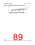
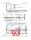
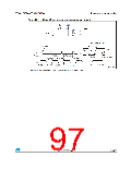
Figure 24. Recommended NRST pin protection
Electrical characteristics
6
$$
%XTERNAL
RESET CIRCUITꢐꢃꢑ
2
05
ꢐꢉꢑ
)NTERNAL 2ESET
.234
&ILTER
ꢄꢏꢃ &
-3ꢃꢅꢁꢆꢁ6ꢃ
1. The reset network protects the device against parasitic resets.
2. The user must ensure that the level on the NRST pin can go below the VIL(NRST) max level specified in
Table 55. Otherwise the reset will not be taken into account by the device.
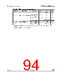
6.3.16
Timer characteristics
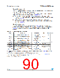
Symbol
Parameter
Conditions
Min
Typ
Max
Unit
0.475VDDA
- 0.2
(1)
VIL(NPOR)
NPOR Input low level voltage
V
0.5VDDA
+ 0.2
(1)
VIH(NPOR)
NPOR Input high level voltage
NPOR Schmitt trigger voltage
hysteresis
(1)
Vhys(NPOR)
200
40
mV
RPU
Weak pull-up equivalent resistor(2)
VIN = VSS
25
55
kΩ
1. Guaranteed by design, not tested in production.
2. The pull-up is designed with a true resistance in series with a switchable PMOS. This PMOS contribution to
the series resistance is minimal (~10% order).
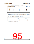
The parameters given in Table 56 are guaranteed by design.
Refer to Section 6.3.14: I/O port characteristics for details on the input/output alternate
function characteristics (output compare, input capture, external clock, PWM output).
(1)
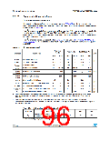
Table 56. TIMx characteristics
Symbol
Parameter
Conditions
Min
Max
Unit
tTIMxCLK
1
-
fTIMxCLK = 72 MHz
(except TIM1/8)
13.9
6.95
-
ns
ns
(2)
Timer resolution time
tres(TIM)
f
TIMxCLK = 144 MHz,
-
x= 1.8
fTIMxCLK/2
0
0
-
MHz
MHz
Timer external clock
frequency on CH1 to CH4
(2)
fEXT
f
TIMxCLK = 72 MHz
36
16
32
TIMx (except TIM2)
TIM2
(2)
Timer resolution
bit
ResTIM
-
Doc ID 023353 Rev 5
93/133

 STMICROELECTRONICS [ ST ]