Electrical characteristics
STM32F302xx/STM32F303xx
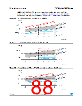
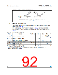
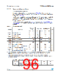
Figure 23. I/O AC characteristics definition
90%
10 %
50%
50%
90%
10%
t
EXTERNAL
OUTPUT
ON 50pF
t
r(IO)out
r(IO)out
T
Maximum frequency is achieved if (t + t ) ≤ 2/3)T and if the duty cycle is (45-55%)
r
f
when loaded by 50pF
ai14131
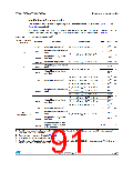
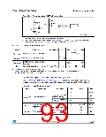
6.3.15
NRST pin characteristics
The NRST pin input driver uses CMOS technology. It is connected to a permanent pull-up
resistor, R (see Table 52).
PU
Unless otherwise specified, the parameters given in Table 55 are derived from tests
performed under ambient temperature and V supply voltage conditions summarized in
DD
Table 22.
Table 55. NRST pin characteristics
Symbol
Parameter
Conditions
Min
Typ
Max
Unit
0.3VDD
+
(1)
VIL(NRST)
NRST Input low level voltage
-
-
0.07(1)
V
0.445VDD
0.398(1)
+
(1)
VIH(NRST)
NRST Input high level voltage
-
-
Vhys(NRST) NRST Schmitt trigger voltage hysteresis
-
25
-
200
-
55
100
-
mV
kΩ
ns
RPU
Weak pull-up equivalent resistor(2)
VIN = VSS
40
-
(1)
VF(NRST)
NRST Input filtered pulse
(1)
VNF(NRST)
NRST Input not filtered pulse
500
-
ns
1. Guaranteed by design, not tested in production.
2. The pull-up is designed with a true resistance in series with a switchable PMOS. This PMOS contribution to the series
resistance must be minimum (~10% order).
92/133
Doc ID 023353 Rev 5

 STMICROELECTRONICS [ ST ]