Electrical characteristics
STM32F302xx/STM32F303xx
Output driving current
The GPIOs (general purpose input/outputs) can sink or source up to +/-8 mA, and sink or
source up to +/- 20 mA (with a relaxed V ).
V
OL/ OH
In the user application, the number of I/O pins which can drive current must be limited to
respect the absolute maximum rating specified in Section 6.2:
●
The sum of the currents sourced by all the I/Os on V
plus the maximum Run
DD,
consumption of the MCU sourced on V
cannot exceed the absolute maximum rating
DD,
IVDD(Σ) (see Table 20).
●
The sum of the currents sunk by all the I/Os on V plus the maximum Run
SS
consumption of the MCU sunk on V cannot exceed the absolute maximum rating
SS
IVSS(Σ) (see Table 20).
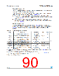
Output voltage levels
Unless otherwise specified, the parameters given in Table 53 are derived from tests
performed under ambient temperature and V supply voltage conditions summarized in
DD
Table 22. All I/Os (FT, TTa and Tc unless otherwise specified) are CMOS and TTL
compliant.
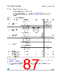
Table 53. Output voltage characteristics
Symbol
Parameter
Conditions
Min
Max
0.4
-
Unit
VOL
Output low level voltage for an I/O pin
Output high level voltage for an I/O pin
Output low level voltage for an I/O pin
Output high level voltage for an I/O pin
CMOS port(2)
IIO = +8 mA
2.7 V < VDD < 3.6 V
-
(1)
(3)
VOH
VDD–0.4
VOL
TTL port(2)
IIO =+ 8mA
2.7 V < VDD < 3.6 V
-
0.4
-
(1)
(3)
VOH
2.4
(1)(4)
VOL
Output low level voltage for an I/O pin
Output high level voltage for an I/O pin
Output low level voltage for an I/O pin
Output high level voltage for an I/O pin
-
1.3
-
V
I
IO = +20 mA
(3)(4)
2.7 V < VDD < 3.6 V
VOH
VDD–1.3
-
(1)(4)
VOL
0.4
-
I
IO = +6 mA
(3)(4)
2 V < VDD < 2.7 V
VOH
VDD–0.4
Output low level voltage for an FTf I/O pin in
FM+ mode
IIO = +20 mA
2.7 V < VDD < 3.6 V
(1)(4)
VOLFM+
-
0.4
1. The IIO current sunk by the device must always respect the absolute maximum rating specified in Table 20 and the sum of
IIO (I/O ports and control pins) must not exceed ΣIIO(PIN)
.
2. TTL and CMOS outputs are compatible with JEDEC standards JESD36 and JESD52.
3. The IIO current sourced by the device must always respect the absolute maximum rating specified in Table 20 and the sum
of IIO (I/O ports and control pins) must not exceed ΣIIO(PIN)
.
4. Data based on design simulation.
90/133
Doc ID 023353 Rev 5

 STMICROELECTRONICS [ ST ]