STM32F302xx/STM32F303xx
Electrical characteristics
6.3.14
I/O port characteristics
General input/output characteristics
Unless otherwise specified, the parameters given in Table 52 are derived from tests
performed under the conditions summarized in Table 22. All I/Os are CMOS and TTL
compliant.
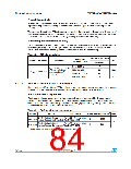
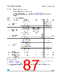
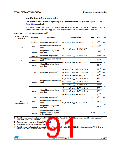
Table 52. I/O static characteristics
Symbol
Parameter
Conditions
Min
Typ
Max
Unit
TC and TTa I/O
FT and FTf I/O
BOOT0
-
-
0.3 VDD+0.07 (1)
0.475 VDD-0.2 (1)
0.3 VDD–0.3 (1)
-
-
Low level input
voltage
VIL
-
-
(2)
All I/Os except BOOT0
TC and TTa I/O
FT and FTf I/O
BOOT0
-
-
0.3 VDD
V
0.445 VDD+0.398 (1)
0.5 VDD+0.2 (1)
0.2 VDD+0.95 (1)
-
-
-
-
-
-
-
-
-
High level input
voltage
VIH
-
(2)
All I/Os except BOOT0
TC and TTa I/O
FT and FTf I/O
BOOT0
0.7 VDD
-
-
-
-
200 (1)
100 (1)
300 (1)
Schmitt trigger
hysteresis
Vhys
mV
TC, FT and FTf I/O
TTa I/O in digital mode
VSS ≤ VIN ≤ VDD
-
-
0.1
TTa I/O in digital mode
-
-
-
-
1
Input leakage
current (3)
VDD ≤ VIN ≤ VDDA
Ilkg
µA
TTa I/O in analog mode
0.2
10
55
VSS ≤ VIN ≤ VDDA
FT and FTf I/O(4)
-
-
VDD ≤ VIN ≤ 5 V
Weak pull-up
RPU
VIN = VSS
VIN = VDD
25
40
kΩ
equivalent resistor(5)
Weak pull-down
RPD
CIO
25
-
40
5
55
-
kΩ
equivalent resistor(5)
I/O pin capacitance
pF
1. Data based on design simulation.
2. Tested in production.
3. Leakage could be higher than the maximum value. if negative current is injected on adjacent pins. Refer to Table 51: I/O
current injection susceptibility.
4. To sustain a voltage higher than VDD +0.3 V, the internal pull-up/pull-down resistors must be disabled.
5. Pull-up and pull-down resistors are designed with a true resistance in series with a switchable PMOS/NMOS. This
PMOS/NMOS contribution to the series resistance is minimum (~10% order).
Doc ID 023353 Rev 5
87/133

 STMICROELECTRONICS [ ST ]