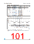
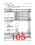
STM32F302xx/STM32F303xx
Electrical characteristics
6.3.18
ADC characteristics
Unless otherwise specified, the parameters given in Table 66 to Table 69 are guaranteed by
design, with conditions summarized in Table 22.
Table 66. ADC characteristics
Symbol
Parameter
Conditions
Min
Typ
Max
Unit
Analog supply voltage for
ADC
VDDA
fADC
2
-
-
-
3.6
72
V
ADC clock frequency
Sampling rate
0.14
0.01
MHz
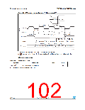
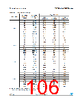
Resolution = 12 bits,
Fast Channel
5.14
Resolution = 10 bits,
Fast Channel
0.012
0.014
0.0175
-
-
-
-
-
6
7.2
9
(1)
fS
MSPS
Resolution = 8 bits,
Fast Channel
Resolution = 6 bits,
Fast Channel
fADC = 72 MHz
Resolution = 12 bits
5.14
MHz
(1)
fTRIG
External trigger frequency
Resolution = 12 bits
-
0
-
-
-
-
14
1/fADC
V
VAIN
Conversion voltage range
External input impedance
VDDA
100
(1)
RAIN
kΩ
Internal sample and hold
capacitor
(1)
CADC
-
5
-
pF
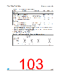
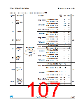
f
ADC = 72 MHz
1.56
112
µs
(1)
tCAL
Calibration time
1/fADC
1/fADC
1/fADC
1/fADC
1/fADC
1/fADC
1/fADC
1/fADC
1/fADC
µs
CKMODE = 00
CKMODE = 01
CKMODE = 10
CKMODE = 11
CKMODE = 00
CKMODE = 01
CKMODE = 10
CKMODE = 11
1.5
2
-
2.5
2
Trigger conversion latency
Regular and injected
channels without conversion
abort
-
(1)
tlatr
-
-
2.25
2.125
3.5
-
-
2.5
3
-
Trigger conversion latency
Injected channels aborting a
regular conversion
-
3
(1)
tlatrinj
-
-
-
3.25
3.125
8.35
601.5
-
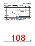
f
ADC = 72 MHz
0.021
1.5
-
(1)
tS
Sampling time
-
1/fADC
ADC Voltage Regulator
Start-up time
TADCVREG
(1)
-
-
-
10
µs
µs
_STUP
fADC = 72 MHz
Resolution = 12 bits
0.19
3.5
Total conversion time
(including sampling time)
(1)
tCONV
14 to 252 (tS for sampling + 12.5 for
successive approximation)
Resolution = 12 bits
1/fADC
1. Data guaranteed by design
Doc ID 023353 Rev 5
105/133

 STMICROELECTRONICS [ ST ]