CONTROLLER AREA NETWORK (bxCAN)
CONTROLLER AREA NETWORK (Cont’d)
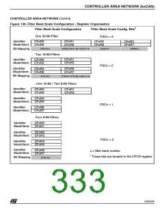
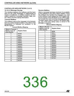
Filter Bank Scale and Mode Configuration
The filter banks are configured by means of the
corresponding CFCRx register. To configure a fil-
ter bank it must be deactivated by clearing the
FACT bit in the CFCR register. The filter scale is
configured by means of the FSC[1:0] bits in the
corresponding CFCR register, refer to Figure 149.
The identifier list or identifier mask mode for the
corresponding Mask/Identifier registers is config-
ured by means of the FMCLx and FMCHx bits in
the CFMR register. The FMCLx bit defines the
mode for the two least significant bytes, and the
FMCHx bit the mode for the two most significant
bytes of filter bank x. Examples:
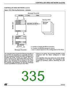
data to the right location the application has to
identify the data by means of the identifier. To
avoid this and to ease the access to the RAM loca-
tions, the CAN controller provides a Filter Match
Index.
This index is stored in the mailbox together with
the message according to the filter priority rules.
Thus each received message has its associated
filter match index.
The Filter Match index can be used in two ways:
– Compare the Filter Match index with a list of ex-
pected values.
– If filter bank 1 is configured as two 16-bit filters,
then the FMCL1 bit defines the mode of the
CF1R2 and CF1R3 registers and the FMCH1 bit
defines the mode of the CF1R6 and CF1R7 reg-
isters.
– Use the Filter Match Index as an index on an ar-
ray to access the data destination location.
For non-masked filters, the software no longer has
to compare the identifier.
If the filter is masked the software reduces the
comparison to the masked bits only.
– If filter bank 2 is configured as four 8-bit filters,
then the FMCL2 bit defines the mode of the
CF2R1 and CF2R3 registers and the FMCH2 bit
defines the mode of the CF2R5 and CF2R7 reg-
isters.
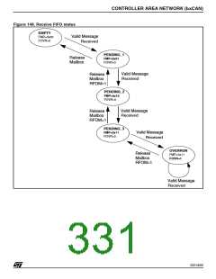
Filter Priority Rules
Depending on the filter combination it may occur
that an identifier passes successfully through sev-
eral filters. In this case the filter match value stored
in the receive mailbox is chosen according to the
following rules:
Note: In 32-bit configuration, the FMCLx and FM-
CHx bits must have the same value to ensure that
the four Mask/Identifier registers are in the same
mode.
– A filter in identifier list mode prevails on an filter
in mask mode.
To filter a group of identifiers, configure the Mask/
Identifier registers in mask mode.
– A filter with full identifier coverage prevails over
filters covering part of the identifier, e.g. 16-bit fil-
ters prevail over 8-bit filters.
To select single identifiers, configure the Mask/
Identifier registers in identifier list mode.
– Filters configured in the same mode and with
identical coverage are prioritized by filter number
and register number. The lower the number the
higher the priority.
Filters not used by the application should be left
deactivated.
Filter Match Index
Once a message has been received in the FIFO it
is available to the application. Typically application
data are copied into RAM locations. To copy the
334/426
9

 STMICROELECTRONICS [ ST ]