CONTROLLER AREA NETWORK (bxCAN)
CONTROLLER AREA NETWORK (Cont’d)
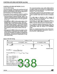
10.10.5.7 Bit Timing
The resynchronization jump width (RJW) defines
an upper bound to the amount of lengthening or
shortening of the bit segments. It is programmable
between 1 and 4 time quanta.
The bit timing logic monitors the serial bus-line and
performs sampling and adjustment of the sample
point by synchronizing on the start-bit edge and re-
synchronizing on the following edges.
A valid edge is defined as the first transition in a bit
time from dominant to recessive bus level provid-
ed the controller itself does not send a recessive
bit.
Its operation may be explained simply by splitting
nominal bit time into three segments as follows:
– Synchronization segment (SYNC_SEG): a bit
change is expected to occur within this time seg-
ment. It has a fixed length of one time quantum
If a valid edge is detected in BS1 instead of
SYNC_SEG, BS1 is extended by up to RJW so
that the sample point is delayed.
(1 x t
).
CAN
Conversely, if a valid edge is detected in BS2 in-
stead of SYNC_SEG, BS2 is shortened by up to
RJW so that the transmit point is moved earlier.
– Bit segment 1 (BS1): defines the location of the
sample point. It includes the PROP_SEG and
PHASE_SEG1 of the CAN standard. Its duration
is programmable between 1 and 16 time quanta
but may be automatically lengthened to compen-
sate for positive phase drifts due to differences in
the frequency of the various nodes of the net-
work.
As a safeguard against programming errors, the
configuration of the Bit Timing Register (BTR) is
only possible while the device is in STANDBY
mode.
Note: for a detailed description of the CAN bit tim-
ing and resynchronization mechanism, please re-
fer to the ISO 11898 standard.
– Bit segment 2 (BS2): defines the location of the
transmit point. It represents the PHASE_SEG2
of the CAN standard. Its duration is programma-
ble between 1 and 8 time quanta but may also be
automatically shortened to compensate for neg-
ative phase drifts.
Figure 152. Bit Timing
NOMINAL BIT TIME
BIT SEGMENT 1 (BS1)
SYNC_SEG
BIT SEGMENT 2 (BS2)
1 x t
t
t
BS2
CAN
BS1
SAMPLE POINT
TRANSMIT POINT
1
BaudRate = -------------------------------------------------
NominalBitTime
NominalBitTime = 1 × tCAN + tBS1 + tBS2
with:
t
t
t
= t
= t
x (TS1[3:0] + 1) ,
x (TS2[2:0] + 1),
x BRP,
BS1
BS2
CAN
CAN
= t
CAN
CPU
CPU
t
= time period of the CPU clock,
BRP = BRP[5:0] + 1 = Baud Rate Prescaler
BRP[5:0] is defined in the CBTR0 Register,
TS1[3:0] and TS2[2:0] are defined in the CBTR1 Register.
338/426
9

 STMICROELECTRONICS [ ST ]