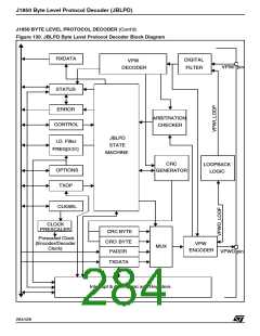
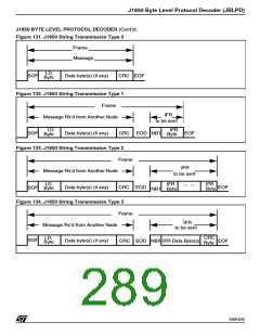
J1850 Byte Level Protocol Decoder (JBLPD)
J1850 BYTE LEVEL PROTOCOL DECODER (Cont’d)
10.9.3 Functional Description
In the case of the reception of an invalid bit, the
JBLPD peripheral will set the IBD bit in the ER-
ROR register. The JBLPD peripheral shall termi-
nate any transmissions in progress, and disable
receive transfers and RDRF flags until the VPW
decoder recognizes a valid EOF symbol from the
bus.
10.9.3.1 J1850 protocol symbols
J1850 symbols are defined as a duration (in micro-
seconds or clock cycles) and a state which can be
either an active state (logic high level on VPWO)
or a passive state (logic low level on VPWO).
An idle J1850 bus is in a passive state.
Any symbol begins by changing the state of the
VPW line. The line is in this state for a specific du-
ration depending on the symbol being transmitted.
The JBLPD’s state machine handles all the Tv
l.D.s in accordance with the SAE J1850 specifica-
tion.
Note: Depending on the value of a control bit, the
polarity of the VPWI input can be the same as the
J1850 bus or inverted with respect to it.
Durations, and hence symbols, are measured as
time between successive state transitions. Each
symbol has only one level transition of a specific
duration.
Symbols for logic zero and one data bits can be ei-
ther a high or a low level, but all other symbols are
defined at only one level.
Table 52. J1850 Symbol definitions
Symbol
Data Bit Zero
Definition
Each symbol is placed directly next to another.
Therefore, every level transition means that anoth-
er symbol has begun.
Passive for Tv1 or Ac-
tive for Tv2
Passive for Tv2 or Ac-
tive for Tv1
Data Bit One
Data bits of a logic zero are either a short duration
if in a passive state or a long duration if in an active
state. Data bits of a logic one are either a long du-
ration if in a passive state or a short duration if in
an active state. This ensures that data logic zeros
predominate during bus arbitration.
Start of Frame (SOF)
End of Data (EOD)
Active for Tv3
Passive for Tv3
Passive for Tv4
Passive for Tv6
Passive for > Tv6
Active for Tv1 or Tv2
Active for Tv5
End of Frame (EOF)
Inter Frame Separation (IFS)
IDLE Bus Condition (IDLE)
Normalization Bit (NB)
Break (BRK)
An eight bit data byte transmission will always
have eight transitions. For all data byte and CRC
byte transfers, the first bit is a passive state and
the last bit is an active state.
For the duration of the VPW, symbols are ex-
pressed in terms of Tv’s (or VPW mode timing val-
ues). J1850 symbols and Tv values are described
in the SAE J1850 specification, in Table 52 and in
Table 53.
Table 53. J1850 VPW Mode Timing Value (Tv)
definitions (in clock cycles)
Pulse Width
or Tv I.D.
Minimum
Duration
Nominal
Duration
Maximum
Duration
An ignored Tv I.D. occurs for level transitions
which occur in less than the minimum time re-
quired for an invalid bit detect. The VPW encoder
does not recognize these characters as they are
filtered out by the digital filter. The VPW decoder
does not resynchronize its counter with either
edge of “ignored” pulses. Therefore, the counter
which times symbols continues to time from the
last transition which occurred after a valid symbol
(including the invalid bit symbol) was recognized.
Ignored
Invalid Bit
Tv1
0
N/A
<=7
>7
N/A
64
<=34
<=96
<=163
<=239
N/A
>34
Tv2
>96
128
200
280
300
300
Tv3
>163
>239
>239
>280
Tv4
Tv5
N/A
A symbol recognized as an invalid bit will resyn-
chronize the VPW decoder to the invalid bit edges.
Tv6
N/A
285/426
9

 STMICROELECTRONICS [ ST ]