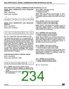
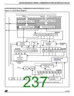
ASYNCHRONOUS SERIAL COMMUNICATIONS INTERFACE (SCI-A)
ASYNCHRONOUS SERIAL COMMUNICATIONS INTERFACE (Cont’d)
10.6.4 Functional Description
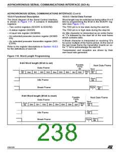
10.6.4.1 Serial Data Format
The block diagram of the Serial Control Interface,
is shown in Figure 117. It contains 6 dedicated
registers:
Word length may be selected as being either 8 or 9
bits by programming the M bit in the SCICR1 reg-
ister (see Figure 117).
– Two control registers (SCICR1 & SCICR2)
– A status register (SCISR)
The TDO pin is in low state during the start bit.
The TDO pin is in high state during the stop bit.
– A baud rate register (SCIBRR)
An Idle character is interpreted as an entire frame
of “1”s followed by the start bit of the next frame
which contains data.
– An extended prescaler receiver register (SCIER-
PR)
A Break character is interpreted on receiving “0”s
for some multiple of the frame period. At the end of
the last break frame the transmitter inserts an ex-
tra “1” bit to acknowledge the start bit.
– An extended prescaler transmitter register (SCI-
ETPR)
Refer to the register descriptions in Section 10.6.5
for the definitions of each bit.
Transmission and reception are driven by their
own baud rate generator.
Figure 118. Word Length Programming
9-bit Word length (M bit is set)
Possible
Next Data Frame
Parity
Data Frame
Bit
Next
Start
Bit
Start
Bit
Stop
Bit
Bit2
Bit6
Bit3
Bit4
Bit5
Bit7
Bit8
Bit0 Bit1
Start
Bit
Idle Frame
Start
Bit
Extra
’1’
Break Frame
8-bit Word length (M bit is reset)
Possible
Parity
Next Data Frame
Data Frame
Bit
Next
Start
Bit
Start
Bit
Stop
Bit
Bit2
Bit6
Bit1
Bit3
Bit4
Bit5
Bit7
Bit0
Start
Bit
Idle Frame
Start
Bit
Extra
’1’
Break Frame
238/426
9

 STMICROELECTRONICS [ ST ]