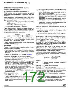
EXTENDED FUNCTION TIMER (EFT)
EXTENDED FUNCTION TIMER (Cont’d)
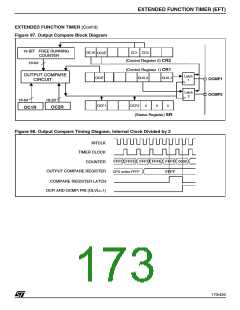
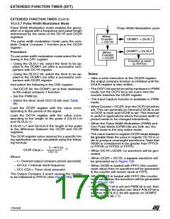
10.3.3.7 Pulse Width Modulation Mode
Pulse Width Modulation mode enables the gener-
ation of a signal with a frequency and pulse length
determined by the value of the OC1R and OC2R
registers.
Pulse Width Modulation cycle
When
Counter
= OC1R
OCMP1 = OLVL1
The pulse width modulation mode uses the com-
plete Output Compare 1 function plus the OC2R
register.
OCMP1 = OLVL2
Procedure
When
Counter
= OC2R
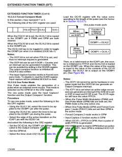
To use pulse width modulation mode select the fol-
lowing in the CR1 register:
Counter is reset
to FFFCh
– Using the OLVL1 bit, select the level to be ap-
plied to the OCMP1 pin after a successful com-
parison with OC1R register.
Notes:
– Using the OLVL2 bit, select the level to be ap-
plied to the OCMP1 pin after a successful com-
parison with OC2R register.
– After a write instruction to the OCiHR register,
the output compare function is inhibited until the
OCiLR register is also written.
And select the following in the CR2 register:
– The OCF1 bit cannot be set by hardware in PWM
mode, but the OCF2 bit is set every time the
counter matches the OC2R register.
– Set OC1E bit: the OCMP1 pin is then dedicated
to the output compare 1 function.
– Set the PWM bit.
– The Input Capture function is available in PWM
mode.
– Select the timer clock CC[1:0] bits (see Table
36).
– When Counter = OC2R, then the OCF2 bit will be
set. This can generate an interrupt if OCIE is set
or OCIE is reset and OC2IE is set. This interrupt
is useful in applications where the pulse-width or
period needs to be changed interactively.
Load the OC2R register with the value corre-
sponding to the period of the signal.
Load the OC1R register with the value corre-
sponding to the length of the pulse if (OLVL1=0
and OLVL2=1).
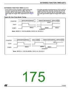
– When the Pulse Width Modulation (PWM) and
One Pulse Mode (OPM) bits are both set, the
PWM mode is the only active mode.
If OLVL1=1 and OLVL2=0 the length of the pulse
is the difference between the OC2R and OC1R
registers.
– The value loaded in register OC2R must always
be greater than the value in register OC1R in or-
der to produce meaningful waveforms. Note that
0000h is considerred to be greater than FFFCh
or FFFDh or FFFEh or FFFFh.
The OCiR register value required for a specific tim-
ing application can be calculated using the follow-
ing formula:
t
INTCLK
*
- 5
OCiR Value =
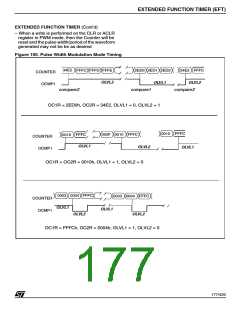
– When OC1R >OC2R, no waveform will be gen-
erated.
CC[1:0]
Where:
– When OC2R = OC1R, a square waveform will
be generated as in Figure 100
– t = Desired output compare period (seconds)
– INTCLK = Internal clock frequency
– When OC2R is loaded with FFFC (the counter
reset value) then no waveform will be generated
& the counter will remain stuck at FFFC.
– CC1-CC0 = Timer clock prescaler
The Output Compare 2 event causes the counter
to be initialized to FFFCh (See Figure 100).
– When OC1R is loaded with FFFC (the counter
reset value) then the waveform will be generated
as in Figure 100
– When FOLV1 bit is set and PWM bit is set, then
PWM mode is the active one. But if FOLV2 bit is
set then the OLVL2 bit will appear on OCMP2
(when OC2E bit = 1).
176/426
9

 STMICROELECTRONICS [ ST ]