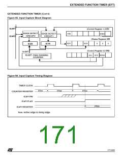
EXTENDED FUNCTION TIMER (EFT)
EXTENDED FUNCTION TIMER (Cont’d)
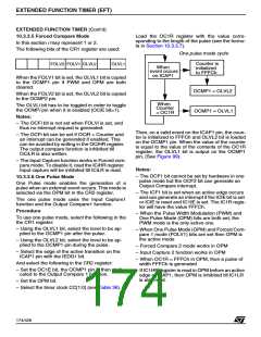
10.3.3.5 Forced Compare Mode
Load the OC1R register with the value corre-
sponding to the length of the pulse (see the formu-
la in Section 10.3.3.7).
In this section i may represent 1 or 2.
The following bits of the CR1 register are used:
One pulse mode cycle
Counter is
initialized
to FFFCh
FOLV2 FOLV1 OLVL2
OLVL1
When
event occurs
on ICAP1
When the FOLV1 bit is set, the OLVL1 bit is copied
to the OCMP1 pin if PWM and OPM are both
cleared.
OCMP1 = OLVL2
OCMP1 = OLVL1
When the FOLV2 bit is set, the OLVL2 bit is copied
to the OCMP2 pin.
When
The OLVLi bit has to be toggled in order to toggle
the OCMPi pin when it is enabled (OCiE bit=1).
Counter
= OC1R
Notes:
– The OCFi bit is not set when FOLVi is set, and
thus no interrupt request is generated.
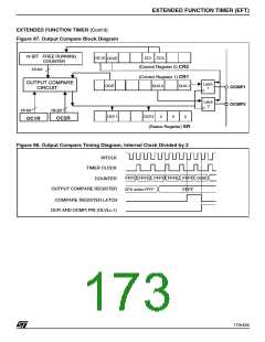
Then, on a valid event on the ICAP1 pin, the coun-
ter is initialized to FFFCh and OLVL2 bit is loaded
on the OCMP1 pin. When the value of the counter
is equal to the value of the contents of the OC1R
register, the OLVL1 bit is output on the OCMP1
pin, (See Figure 99).
– The OCFi bit can be set if OCiR = Counter and
an interrupt can be generated if enabled. This
can be avoided by writing in the OCiHR register.
The output compare function is inhibited till
OCiLR is also written.
– The Input Capture function works in Forced com-
pare mode. To disable it, read the ICiHR register.
Input capture will be inhibited till ICiLR is read.
Notes:
– The OCF1 bit cannot be set by hardware in one
pulse mode but the OCF2 bit can generate an
Output Compare interrupt.
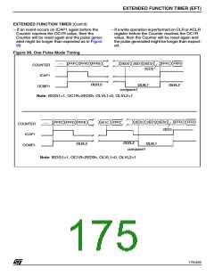
10.3.3.6 One Pulse Mode
One Pulse mode enables the generation of a
pulse when an external event occurs. This mode is
selected via the OPM bit in the CR2 register.
– The ICF1 bit is set when an active edge occurs
and can generate an interrupt if the ICIE bit is set
or ICIE is reset and IC1IE is set. The IC1R regis-
ter will have the value FFFCh.
The one pulse mode uses the Input Capture1
function and the Output Compare1 function.
Procedure
– When the Pulse Width Modulation (PWM) and
One Pulse Mode (OPM) bits are both set, the
PWM mode is the only active one.
To use one pulse mode, select the following in the
the CR1 register:
– Using the OLVL1 bit, select the level to be ap-
plied to the OCMP1 pin after the pulse.
– When One Pulse Mode (OPM) and Forced Com-
pare 1 mode (FOLV1) bits are set then OPM is
the active mode
– Using the OLVL2 bit, select the level to be ap-
plied to the OCMP1 pin during the pulse.
– Forced Compare 2 mode works in OPM
– Input Capture 2 function works in OPM
– Select the edge of the active transition on the
ICAP1 pin with the IEDG1 bit.
– When OC1R = FFFCh in OPM, then a pulse of
width FFFCh is generated
And select the following in the CR2 register:
– Set the OC1E bit, the OCMP1 pin is then dedi-
cated to the Output Compare 1 function.
– If IC1HR register is read in OPM before an active
edge of ICAP1, then OPM is inhibited till IC1LR
is also read.
– Set the OPM bit.
– Select the timer clock CC[1:0] (see Table 36).
174/426
9

 STMICROELECTRONICS [ ST ]