ST40RA
5 System configuration
5.5
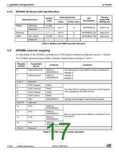
EMI DACK mapping
For full details of the EMI bank address and bank type mappings refer to ST40 System Architecture
Manual Volume 2: Bus Interfaces.
Two DACK strobes are supported in this implementation and are mapped as follows:
●
●
DACK[0]: asserted when a transfer from GPDMA channel[1] occurs to an EMI bank configured
as a MPX device,
DACK[1]: asserted when a transfer from GPDMA channel[2] occurs to an EMI bank configured
as a MPX device.
5.6
EMI address pin mapping
The data width of a connected device is 8, 16 or 32 bits wide. The 16-bit bank must use EDQM3 as
address 1, the LSB address for the device and the 8-bit bank must use EDQM3 as address 1 and
EDQM2 as address 0.
See the ST40 System Architecture Manual, Volume 2: Bus Interfaces for details of setting the
device type and port size using the EMI configuration registers.
Device type
Port size
Device address 25 to 2
Device address 1
Device address 0
SDRAM
Peripheral
SFlash
32-bit
16-bit
8-bit
-
EADDR[25:2]
EADDR[24:2]
EADDR[23:2]
EADDR[25:2]
-
-
-
EDQM3
EDQM3
-
EDQM2
-
MPX
Table 7: Mapping the internal address lines of a connected device
ADCS 7260755H
STMicroelectronics
18/94

 STMICROELECTRONICS [ ST ]