ST24E16, ST25E16
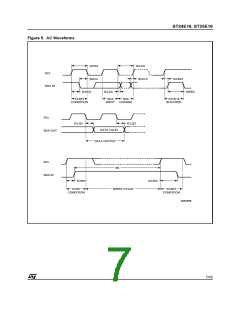
Table 7. AC Characteristics
(TA = 0 to 70 °C or –40 to 85 °C; VCC = 4.5V to 5.5V or 2.5V to 5.5V)
Symbol
tCH1CH2
tCL1CL2
Alt
tR
Parameter
Min
Max
300
300
300
300
Unit
ns
Clock Rise Time
Clock Fall Time
SDA Rise Time
SDA Fall Time
tF
ns
(1)
tDH1DH2
tR
20
20
ns
(1)
tDL1DL1
tF
ns
(2)
tCHDX
tCHCL
tDLCL
tCLDX
tCLCH
tDXCX
tCHDH
tDHDL
tSU:STA
tHIGH
tHD:STA
tHD:DAT
tLOW
tSU:DAT
tSU:STO
tBUF
tAA
Clock High to Input Transition
Clock Pulse Width High
600
600
600
0
ns
ns
Input Low to Clock Low (START)
Clock Low to Input Transition
Clock Pulse Width Low
ns
µs
µs
ns
1.3
100
600
1.3
200
200
Input Transition to Clock Transition
Clock High to Input High (STOP)
Input High to Input Low (Bus Free)
Clock Low to Next Data Out Valid
Data Out Hold Time
ns
µs
ns
(3)
tCLQV
tCLQX
fC
1000
tDH
ns
fSCL
tWR
Clock Frequency
400
10
kHz
ms
tW
Write Time
Notes: 1. Sampled only, not 100% tested.
2. For a reSTART condition, or following a write cycle.
3. The minimum value delays the falling/rising edge of SDA away from SCL = 1 in order to avoid unwanted START and/or STOP
conditions.
Table 8. AC Measurement Conditions
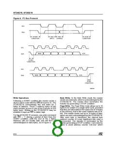
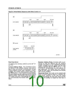
DEVICE OPERATION (cont’d)
Memory Addressing. A data byte in the memory
is addressed through 2 bytes of address informa-
tion. The Most Significant Byte is sent first and the
Least significant Byte is sent after. The Least Sig-
nificant Byte addresses a block of 256 bytes, bits
b10,b9,b8 of the Most Significant Byte select one
block among 8 blocks (one block is 256 bytes).
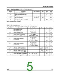
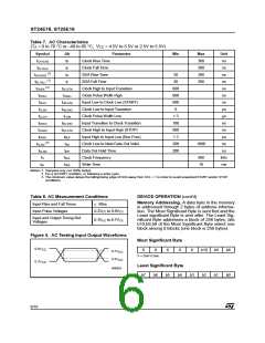
Input Rise and Fall Times
Input Pulse Voltages
≤ 50ns
0.2VCC to 0.8VCC
Input and Output Timing Ref.
Voltages
0.3VCC to 0.7VCC
Figure 4. AC Testing Input Output Waveforms
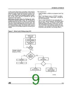
Most Significant Byte
0.8V
CC
X
X
X
X
X
b10
b2
b9
b1
b8
b0
0.7V
CC
X = Don’t Care.
0.3V
CC
0.2V
CC
Least Significant Byte
AI00825
b7
b6
b5
b4
b3
6/16

 STMICROELECTRONICS [ ST ]