ST24E16, ST25E16
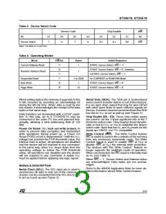
Table 3. Device Select Code
Device Code
Chip Enable
RW
b0
Bit
b7
1
b6
0
b5
1
b4
0
b3
b2
b1
Device Select
E2
E1
E0
RW
Note: The MSB b7 is sent first.
Table 4. Operating Modes
Mode
RW bit
’1’
Bytes
Initial Sequence
Current Address Read
1
1
START, Device Select, RW = ’1’
START, Device Select, RW = ’0’, Address,
reSTART, Device Select, RW = ’1’
As CURRENT or RANDOM Mode
START, Device Select, RW = ’0’
START, Device Select, RW = ’0’
’0’
Random Address Read
’1’
Sequential Read
Byte Write
’1’
1 to 2048
’0’
1
Page Write
’0’
16
When writing data to the memory it responds to the
8 bits received by asserting an acknowledge bit
during the 9th bit time. When data is read by the
bus master, it acknowledges the receipt of the data
bytes in the same way.
Serial Data (SDA). The SDA pin is bi-directional
and is used to transfer data in or out of the memory.
It is an open drain output that may be wire-OR’ed
with other open drain or open collector signals on
the bus. Aresistor must be connected fromthe SDA
bus line to VCC to act as pull up (see Figure 3).
Data transfers are terminated with a STOP condi-
tion. In this way, up to 8 ST24/25E16 may be
connected to the same I2C bus and selected indi-
vidually, allowing a total addressing field of 128
Kbit.
Chip Enable (E0 - E2). These chip enable inputs
are used to set the 3 least significant bits of the 7
bit device select code. They may be driven dynami-
cally or tied to VCC or VSS to establish the device
select code. Note that the VIL and VIH levels for the
inputs are CMOS, not TTL compatible.
Power On Reset: VCC lock out write protect. In
order to prevent data corruption and inadvertent
write operations during power up, a Power On
Reset (POR) circuit is implemented. Untill the VCC
voltage has reached the POR threshold value, the
internal reset is active: all operations are disabled
and the device will not respond to any command.
In the same way, when VCC drops down from the
operating voltage to below the POR threshold
value, all operations are disabled and the device
will not respond to any command. A stable VCC
must be applied before applying any logic signal.
Write Control (WC). The Write Control feature
WC is useful to protect the contents of the memory
from any erroneous erase/write cycle. The Write
Control signal is used to enable (WC at VIH) or
disable (WC at VIL) the internal write protection.
The devices with this Write Control feature no
longer supports the multibyte mode of operation.
When unconnected, the WC input is internally read
as VIL (see Table 5).
When WC = ’1’, Device Select and Address bytes
are acknowledged; Data bytes are not acnowl-
edged.
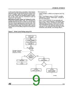
SIGNALS DESCRIPTION
Refer to the AN404 Application Note for more de-
tailed information about Write Control feature.
Serial Clock (SCL). The SCL input pin is used to
synchronize all data in and out of the memory. A
resistor can be connected from the SCL line to VCC
to act as a pull up (see Figure 3)
3/16

 STMICROELECTRONICS [ ST ]