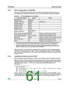
ST10F276E
Bootstrap loader
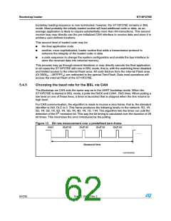
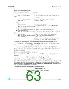
5.4.6
Computing the baud rate error
Considering the following conditions, a computation of the error is given as an example.
●
CPU frequency: 20 MHz
●
Target Bit Rate: 1 Mbit/s
In these conditions, the content of PT0 timer for 29 bits should be:
29 × Fcpu
29 × 20 × 6
[PT0] = --------------------------= ---------------------------- = 580
BitRate
6
1 × 10
Therefore:
This gives:
574 < [PT0] < 586
BRP = 0
tq = 100 ns
Computation of 1 + Tseg1 + Tseg2: Considering the equation:
[PT0] = 58 x (1 + BRP) x (1 + Tseg1 + Tseg2)
Thus:
574
---------
586
58
9 =
≤ Tseg1 + Tseg2 ≤ --------- = 10
58
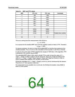
In the algorithm, a rounding up to the superior value is made if the remainder of the division
is greater than half of the divisor. This would have been the case if the PT0 content was 574.
Thus, in this example the result is 1 + Tseg1 + Tseg2 = 10, giving a bit time of exactly 1μs
=> no error in bit rate.
Note:
In most cases (24 MHz, 32 MHz, 40 MHz of CPU frequency and 125, 250, 500 or 1Mb/s of
bit rate), there is no error. Nevertheless, it is better to check for an error with the real
application parameters.
The content of the bit timing register is: 0x1640. This gives a sample point at 80%.
Note:
The (Re)Synchronization Jump Width is fixed to 2 time quanta.
5.4.7
Bootstrap via CAN
After the bootstrap phase, the ST10F276E CAN module is configured as follows:
●
●
●
The pin P4.6 is configured as output (the latch value is ‘1’ = recessive) to assume
CAN1_TxD function.
The MO2 is configured to output the acknowledge of the bootstrap with the standard
identifier E6h, a DLC of 3 and Data0 = D5h, Data1 and 2 = IDCHIP.
The MO1 is configured to receive messages with the standard identifier 5h. Its
acceptance mask is set to ensure that all bits match. The DLC received is not checked:
The ST10 expects only 1 byte of data at a time.
No other message is sent by the ST10F276E after the acknowledge.
Note:
The CAN boot waits for 128 bytes of data instead of 32 bytes (see UART boot). This is done
to allow the User to reconfigure the CAN bit rate as soon as possible.
Doc ID 12303 Rev 3
65/235

 STMICROELECTRONICS [ ST ]