Internal Flash memory
ST10F276E
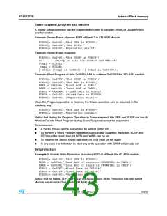
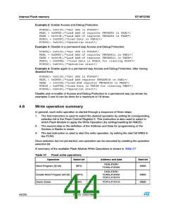
Example 2: Enable Access and Debug Protection.
FCR0H|= 0x0100;/*Set SPR in FCR0H*/
FARL = 0xDFB8;/*Load Add of register FNVAPR0 in FARL*/
FARH = 0x000E;/*Load Add of register FNVAPR0 in FARH*/
FDR0L = 0xFFFC;/*Load Data in FDR0L*/
FCR0H|= 0x8000;/*Operation start*/
Example 3: Disable in a permanent way Access and Debug Protection.
FCR0H|= 0x0100;/*Set SPR in FCR0H*/
FARL = 0xDFBC;/*Load Add of register FNVAPR1L in FARL*/
FARH = 0x000E;/*Load Add of register FNVAPR1L in FARH*/
FDR0L = 0xFFFE; /*Load Data in FDR0L for clearing PDS0*/
FCR0H|= 0x8000;/*Operation start*/
Example 4: Enable again in a permanent way Access and Debug Protection, after having
disabled them.
FCR0H|= 0x0100;/*Set SPR in FCR0H*/
FARL = 0xDFBC;/*Load Add register FNVAPR1H in FARL*/
FARH = 0x000E;/*Load Add register FNVAPR1H in FARH*/
FDR0H = 0xFFFE;/*Load Data in FDR0H for clearing PEN0*/
FCR0H|= 0x8000;/*Operation start*/
Disable and re-enable of Access and Debug Protection in a permanent way (as shown by
examples 3 and 4) can be done for a maximum of 16 times.
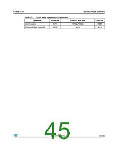
4.6
Write operation summary
In general, each write operation is started through a sequence of three steps:
1. The first instruction is used to select the desired operation by setting its corresponding
selection bit in the Flash Control Register 0. This instruction is also used to select in
which Flash Module to apply the Write Operation (by setting/resetting bit SMOD).
2. The second step is the definition of the Address and Data for programming or the
Sectors or Banks to erase.
3. The last instruction is used to start the write operation, by setting the start bit WMS in
the FCR0.
Once selected, but not yet started, one operation can be canceled by resetting the operation
selection bit.
A summary of the available Flash Module Write Operations is shown in Table 27.
Table 27. Flash write operations
Operation
Select bit
Address and data
Start bit
FARL/FARH
FDR0L/FDR0H
Word Program (32-bit)
WPG
WMS
FARL/FARH
FDR0L/FDR0H
FDR1L/FDR1H
Double Word Program (64-bit)
Sector Erase
DWPG
SER
WMS
WMS
FCR1L/FCR1H
44/235
Doc ID 12303 Rev 3

 STMICROELECTRONICS [ ST ]