ST10F276E
Introduction
1
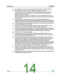
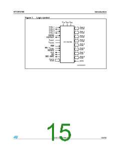
Introduction
The ST10F276E is a derivative of the STMicroelectronics® ST10 family of 16-bit single-chip
CMOS microcontrollers. It combines high CPU performance (up to 32 million instructions
per second) with high peripheral functionality and enhanced I/O-capabilities. It also provides
on-chip high-speed single voltage Flash memory, on-chip high-speed RAM, and clock
generation via PLL.
ST10F276E is processed in 0.18 µm CMOS technology. The MCU core and the logic is
supplied with a 5V to 1.8V on-chip voltage regulator. The part is supplied with a single 5V
supply and I/Os work at 5V.
The device is upward compatible with the ST10F269 device, with the following set of
differences:
●
●
Flash control interface is now based on STMicroelectronics third generation of stand-
alone Flash memories (M29F400 series), with an embedded Program/Erase Controller.
This completely frees up the CPU during programming or erasing the Flash.
Only one supply pin (ex DC1 in ST10F269, renamed into V18) on the QFP144 package
is used for decoupling the internally generated 1.8V core logic supply. Do not connect
this pin to 5.0V external supply. Instead, this pin should be connected to a decoupling
capacitor (ceramic type, typical value 10nF, maximum value 100nF).
●
The AC and DC parameters are modified due to a difference in the maximum CPU
frequency.
●
●
A new VDD pin replaces DC2 of ST10F269.
EA pin assumes a new alternate functionality: it is also used to provide a dedicated
power supply (see VSTBY) to maintain biased a portion of the XRAM (16 Kbytes) when
the main Power Supply of the device (VDD and consequently the internally generated
V18) is turned off for low power mode, allowing data retention. VSTBY voltage shall be in
the range 4.5-5.5 Volt, and a dedicated embedded low power voltage regulator is in
charge to provide the 1.8V for the RAM, the low-voltage section of the 32 kHz oscillator
and the Real-Time Clock module when not disabled. It is allowed to exceed the upper
limit up to 6V for a very short period of time during the global life of the device, and
exceed the lower limit down to 4V when RTC and 32kHz on-chip oscillator are not
used.
●
●
●
A second SSC mapped on the XBUS is added (SSC of ST10F269 becomes here
SSC0, while the new one is referred as XSSC or simply SSC1). Note that some
restrictions and functional differences due to the XBUS peculiarities are present
between the classic SSC, and the new XSSC.
A second ASC mapped on the XBUS is added (ASC0 of ST10F269 remains ASC0,
while the new one is referred as XASC or simply as ASC1). Note that some restrictions
and functional differences due to the XBUS peculiarities are present between the
classic ASC, and the new XASC.
A second PWM mapped on the XBUS is added (PWM of ST10F269 becomes here
PWM0, while the new one is referred as XPWM or simply as PWM1). Note that some
restrictions and functional differences due to the XBUS peculiarities are present
between the classic PWM, and the new XPWM.
●
●
An I2C interface on the XBUS is added (see X-I2C or simply I2C interface).
CLKOUT function can output either the CPU clock (like in ST10F269) or a software
programmable prescaled value of the CPU clock.
Doc ID 12303 Rev 3
13/235

 STMICROELECTRONICS [ ST ]