M41T00
M41T00 clock operation
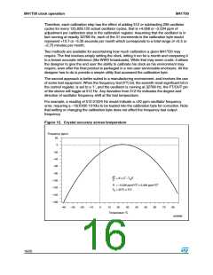
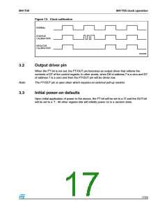
Figure 13. Clock calibration
NORMAL
POSITIVE
CALIBRATION
NEGATIVE
CALIBRATION
AI00594B
3.2
Output driver pin
When the FT bit is not set, the FT/OUT pin becomes an output driver that reflects the
contents of D7 of the control register. In other words, when D6 of address 7 is a zero and D7
of address 7 is a zero and then the FT/OUT pin will be driven low.
Note:
The FT/OUT pin is open drain which requires an external pull-up resistor.
3.3
Initial power-on defaults
Upon initial application of power to the device, the FT bit will be set to a '0' and the OUT bit
will be set to a '1'. All other register bits will initially power on in a random state.
17/25

 STMICROELECTRONICS [ ST ]