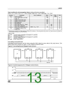
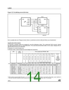
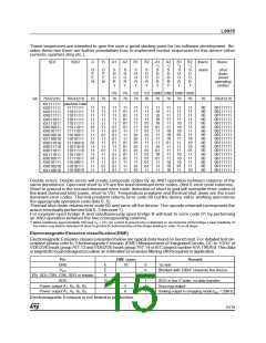
L9935
Serial Data Interface (SPI)
The serial data interface itself consists of the pins SCL (serial clock), SDI (serial data input) and SDO
(serial data output).
To especially support bus controlled applications the additional signals EN (chip enable not) and CSN
(chip select not) are available.
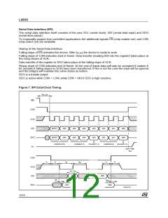
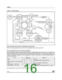
Startup of the Serial Data Interface
Falling slope of EN activates the device. After ten.sck the device is ready to work.
Falling slope of CSN indicates start of frame. Data transfer (reading SDI into the register) takes place at
the rising slopes of SCK.
Data transfer of the register to SDO takes place at the falling slope of SCK.
Rising slope of CSN indicates end of frame. At the end of frame data will only be accepted if modulo 8
bit (modulo8 falling slopes to SCK) have been transferred. If this is not the case the input will be ignored
and the bridges will maintain the same status as before.
SDO is a tristate output.
SDO is active while CSN = LOW, while CSN = HIGH SDO is high resistive.
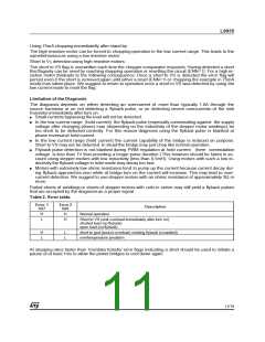
Figure 7. SPI Data/Clock Timing.
t
en_sck
EN
CSN
SCK
SDI
MSB7
MSB7
bit6
bit6
bit5
bit5
bit4
bit4
bit3
bit2
bit2
bit1
bit1
bit0
SDO
bit3
bit0
ERROR BITS
CURRENT A
POLARITY A
CURRENT B
POLARITY B
A
X
t
Pd
CSN
SCK
SDI
t
t
1
t
cl
t
ch
t
t
1
1
1
t
t
su sh
bit7
bit0
td
t
zch
bit7
bit0
SDO
D99AT437
12/19

 STMICROELECTRONICS [ ST ]