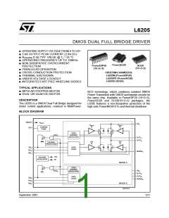
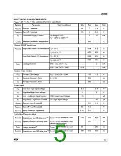
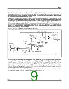
L6205
ELECTRICAL CHARACTERISTICS
(T = 25 °C, V = 48V, unless otherwise specified)
amb
Symbol
s
Parameter
Turn-on Threshold
Test Conditions
Min
6.6
5.6
Typ
7
Max
7.4
6.4
10
Unit
V
V
Sth(ON)
V
Turn-off Threshold
6
V
Sth(OFF)
I
S
Quiescent Supply Current
All Bridges OFF;
T = -25°C to 125°C
5
mA
(7)
j
T
Thermal Shutdown Temperature
165
°C
j(OFF)
Output DMOS Transistors
High-Side Switch ON Resistance T = 25 °C
R
DS(ON)
0.34
0.53
0.4
Ω
Ω
j
(7)
(7)
0.59
T =125 °C
j
Low-Side Switch ON Resistance T = 25 °C
0.28
0.47
0.34
0.53
Ω
Ω
j
T =125 °C
j
I
Leakage Current
EN = Low; OUT = V
2
mA
mA
DSS
S
EN = Low; OUT = GND
-0.15
Source Drain Diodes
V
Forward ON Voltage
I
= 2.8A, EN = LOW
1.15
300
200
1.3
V
SD
SD
t
Reverse Recovery Time
Forward Recovery Time
I = 2.8A
f
ns
ns
rr
t
fr
Logic Input
V
Low level logic input voltage
High level logic input voltage
Low Level Logic Input Current
High Level Logic Input Current
Turn-on Input Threshold
-0.3
2
0.8
7
V
V
IL
IH
IL
V
I
GND Logic Input Voltage
7V Logic Input Voltage
-10
µA
µA
V
I
IH
10
V
1.8
1.3
0.5
2.0
th(ON)
V
V
Turn-off Input Threshold
0.8
V
th(OFF)
th(HYS)
Input Threshold Hysteresis
0.25
V
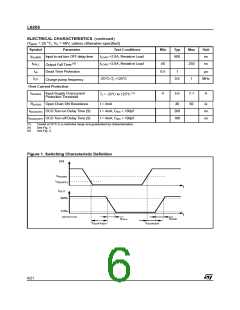
Switching Characteristics
(8)
t
I
I
=2.8A, Resistive Load
=2.8A, Resistive Load
100
250
1.6
400
ns
µs
D(on)EN
LOAD
Enable to out turn ON delay time
t
Input to out turn ON delay time
D(on)IN
LOAD
(dead time included)
(8)
t
I
=2.8A, Resistive Load
=2.8A, Resistive Load
40
250
800
ns
ns
RISE
LOAD
LOAD
Output rise time
(8)
t
I
300
550
D(off)EN
Enable to out turn OFF delay time
5/21

 STMICROELECTRONICS [ ST ]