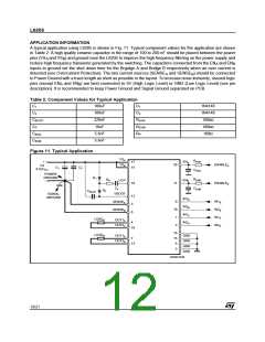
L6205
CIRCUIT DESCRIPTION
POWER STAGES and CHARGE PUMP
The L6205 integrates two independent Power MOS
Full Bridges. Each Power MOS has an Rd-
son=0.3ohm (typical value @ 25°C), with intrinsic
fast freewheeling diode. Cross conduction protection
(collector) structure, a pull-up resistor R and a ca-
EN
pacitor C are connected as shown in Fig. 5. If the
EN
driver is a standard Push-Pull structure the resistor
R
EN
and the capacitor C are connected as shown
EN
is achieved using a dead time (td = 1
µ
s typical) be-
in Fig. 6. The resistor R
should be chosen in the
EN
tween the switch off and switch on of two Power MOS
in one leg of a bridge.
range from 2.2k
Ω
to 180K
Ω
. Recommended values
and 5.6nF.
for R and C are respectively 100K
Ω
EN
EN
Using N Channel Power MOS for the upper transis-
tors in the bridge requires a gate drive voltage above
the power supply voltage. The Bootstrapped (Vboot)
supply is obtained through an internal Oscillator and
few external components to realize a charge pump
circuit as shown in Figure 3. The oscillator output
(VCP) is a square wave at 600kHz (typical) with 10V
amplitude. Recommended values/part numbers for
the charge pump circuit are shown in Table1.
More information on selecting the values is found in
the Overcurrent Protection section.
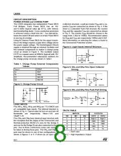
Figure 4. Logic Inputs Internal Structure
5V
ESD
PROTECTION
D01IN1329
Table 1. Charge Pump External Components
Values
Figure 5. EN and EN Pins Open Collector
A
B
C
C
R
220nF
10nF
BOOT
Driving
P
P
5V
5V
100Ω
REN
D1
D2
1N4148
1N4148
OPEN
COLLECTOR
OUTPUT
ENA or ENB
CEN
Figure 3. Charge Pump Circuit
D02IN1349
VS
Figure 6. EN and EN Pins Push-Pull Driving
A
B
D1
D2
CBOOT
5V
RP
CP
REN
ENA or ENB
CEN
PUSH-PULL
OUTPUT
D01IN1328
VCP
VBOOT
VSA VSB
D02IN1350
LOGIC INPUTS
Pins IN1 , IN2 , IN1 and IN2 are TTL/CMOS and
A
A
B
B
µ
C compatible logic inputs. The internal structure is
TRUTH TABLE
INPUTS
shown in Fig. 4. Typical value for turn-on and turn-off
thresholds are respectively Vthon=1.8V and
Vthoff=1.3V.
OUTPUTS
EN
L
IN1
X
IN2
X
OUT1
OUT2
High Z
GND
GND
Vs
Pins EN and EN have identical input structure with
A
B
High Z
GND
Vs
the exception that the drains of the Overcurrent and
thermal protection MOSFETs (one for the Bridge A
and one for the Bridge B) are also connected to these
pins. Due to these connections some care needs to
H
L
L
H
H
L
H
L
H
GND
Vs
H
H
H
Vs
be taken in driving these pins. The EN and EN in-
A
B
X
= Don't care
puts may be driven in one of two configurations as
shown in figures 5 or 6. If driven by an open drain
High Z = High Impedance Output
8/21

 STMICROELECTRONICS [ ST ]