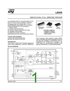
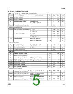
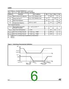
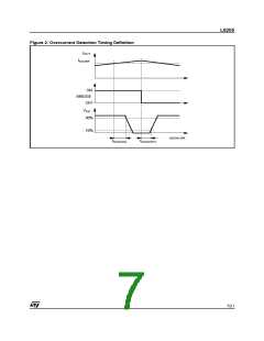
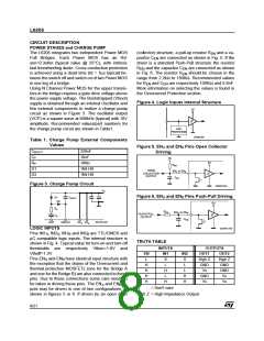
L6205
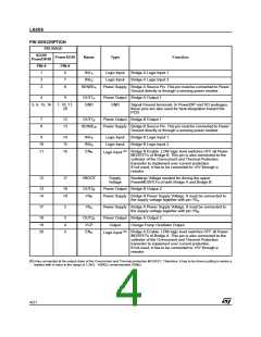
PIN DESCRIPTION
PACKAGE
SO20/
PowerDIP20
PowerSO20
Name
Type
Function
PIN #
PIN #
1
2
3
6
7
8
IN1
IN2
Logic Input
Logic Input
Bridge A Logic Input 1.
Bridge A Logic Input 2.
A
A
SENSE
Power Supply Bridge A Source Pin. This pin must be connected to Power
Ground directly or through a sensing power resistor.
A
4
9
OUT1
Power Output Bridge A Output 1.
A
5, 6, 15, 16
1, 10, 11,
20
GND
GND
Signal Ground terminals. In PowerDIP and SO packages,
these pins are also used for heat dissipation toward the
PCB.
7
8
12
13
OUT1
Power Output Bridge B Output 1.
B
SENSE
Power Supply Bridge B Source Pin. This pin must be connected to Power
Ground directly or through a sensing power resistor.
B
9
14
15
16
IN1
IN2
Logic Input
Logic Input
Bridge B Logic Input 1.
Bridge B Logic Input 2.
B
B
B
10
11
(6)
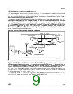
EN
Bridge B Enable. LOW logic level switches OFF all Power
MOSFETs of Bridge B. This pin is also connected to the
collector of the Overcurrent and Thermal Protection
transistor to implement over current protection.
If not used, it has to be connected to +5V through a
resistor.
Logic Input
12
17
VBOOT
OUT2
Supply
Voltage
Bootstrap Voltage needed for driving the upper
PowerMOSFETs of both Bridge A and Bridge B.
13
14
18
19
Power Output Bridge B Output 2.
B
VS
Power Supply Bridge B Power Supply Voltage. It must be connected to
B
the supply voltage together with pin VS .
A
17
2
VS
Power Supply Bridge A Power Supply Voltage. It must be connected to
A
the supply voltage together with pin VS .
B
18
19
20
3
4
5
OUT2
VCP
Power Output Bridge A Output 2.
A
Output
Charge Pump Oscillator Output.
(6)
EN
Bridge A Enable. LOW logic level switches OFF all Power
MOSFETs of Bridge A. This pin is also connected to the
collector of the Overcurrent and Thermal Protection
transistor to implement over current protection.
If not used, it has to be connected to +5V through a
resistor.
A
Logic Input
(6) Also connected at the output drain of the Overcurrent and Thermal protection MOSFET. Therefore, it has to be driven putting in series a
resistor with a value in the range of 2.2kΩ - 180KΩ, recommended 100kΩ
4/21

 STMICROELECTRONICS [ ST ]