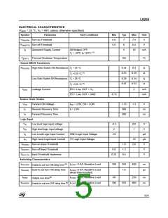
L6205
NON-DISSIPATIVE OVERCURRENT PROTECTION
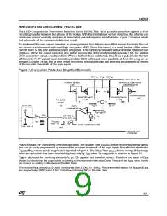
The L6205 integrates an Overcurrent Detection Circuit (OCD). This circuit provides protection against a short
circuit to ground or between two phases of the bridge. With this internal over current detection, the external cur-
rent sense resistor normally used and its associated power dissipation are eliminated. Figure 7 shows a simpli-
fied schematic of the overcurrent detection circuit.
To implement the over current detection, a sensing element that delivers a small but precise fraction of the out-
put current is implemented with each high side power MOS. Since this current is a small fraction of the output
current there is very little additional power dissipation. This current is compared with an internal reference cur-
rent I
. When the output current in one bridge reaches the detection threshold (typically 5.6A) the relative
REF
OCD comparator signals a fault condition. When a fault condition is detected, the EN pin is pulled below the turn
off threshold (1.3V typical) by an internal open drain MOS with a pull down capability of 4mA. By using an ex-
ternal R-C on the EN pin, the off time before recovering normal operation can be easily programmed by means
of the accurate thresholds of the logic inputs.
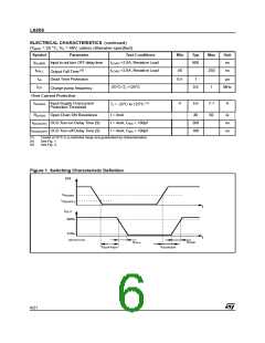
Figure 7. Overcurrent Protection Simplified Schematic
OUT1A VSA OUT2A
POWER SENSE
1 cell
HIGH SIDE DMOSs OF
THE BRIDGE A
I1A
I2A
POWER SENSE
1 cell
POWER DMOS
n cells
POWER DMOS
n cells
TO GATE
LOGIC
+
µC or LOGIC
I1A / n
I2A / n
OCD
COMPARATOR
+5V
(I1A+I2A) / n
IREF
REN
CEN
ENA
INTERNAL
OPEN-DRAIN
RDS(ON)
40Ω TYP.
OVER TEMPERATURE
D02IN1353
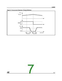
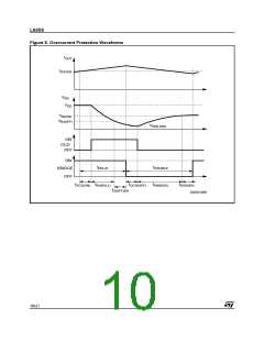
Figure 8 shows the Overcurrent Detection operation. The Disable Time t
before recovering normal opera-
DISABLE
tion can be easily programmed by means of the accurate thresholds of the logic inputs. It is affected whether by
C
EN
and R values and its magnitude is reported in Figure 9. The Delay Time t before turning off the bridge
EN
DELAY
when an overcurrent has been detected depends only by C value. Its magnitude is reported in Figure 10.
EN
C
EN
is also used for providing immunity to pin EN against fast transient noises. Therefore the value of C
EN
should be chosen as big as possible according to the maximum tolerable Delay Time and the R value should
EN
be chosen according to the desired Disable Time.
The resistor R should be chosen in the range from 2.2K
Ω
to 180K
Ω. Recommended values for R and C
EN EN
EN
are respectively 100K
Ω and 5.6nF that allow obtaining 200µs Disable Time.
9/21

 STMICROELECTRONICS [ ST ]