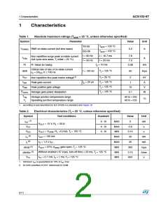
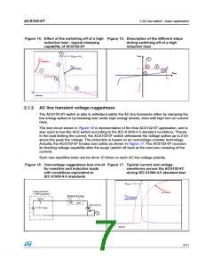
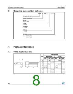
ACS102-6T
1 Characteristics
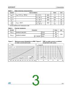
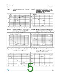
Figure 7. On-state characteristics (maximal
values)
Figure 8. SO-8 junction to ambient thermal
resistance versus copper surface
under tab (PCB FR4, copper
thickness 35 µm)
I
TM(A)
10.00
1.00
0.10
0.01
160
140
120
100
80
Tj max.:
to= 0.8 V
Rd= 500 mΩ
SO-8
V
Tj=125°C
Tj=25°C
60
40
20
SCU(mm²)
VTM(V)
2.0
0
0
50
100
150
200
250
300
0.0
0.5
1.0
1.5
2.5
3.0
3.5
4.0
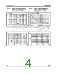
Figure 9. Relative variation of critical rate of Figure 10. Relative variation of critical rate of
decrease of main current (di/dt)c
versus junction temperature
decrease of main current (di/dt)c vs
(dV/dt)c, with turn-off time < 20 ms
(dI/dt)c [ (dV/dt)c ] / Specified (dI/dt)c
(dI/dt)c [Tj] / (dI/dt)c [Tj=125 °C]
2.0
1.8
1.6
1.4
1.2
1.0
0.8
0.6
0.4
0.2
0.0
20
18
16
14
12
10
8
Vout = 400 V
Vout = 400 V
6
4
(dV/dt)c (V/µs)
2
Tj (°C)
0
55
65
75
85
95
105
115
125
0.1
1
10
100
Figure 11. Relative variation of static dV/dt
versus junction temperature
Figure 12. Relative variation of the maximal
clamping voltage versus junction
temperature (min value)
VCL [Tj] / VDRM
C]
T =125°
] / dV/dt [
dV/dt [Tj
j
8
7
6
5
4
3
2
1
0
1.20
1.10
1.00
0.90
0.80
0.70
0.60
0.50
Vout=400V
Tj(°C)
75
Tj(°C)
25
50
100
125
-25
0
25
50
75
100
125
5/11

 STMICROELECTRONICS [ ST ]