16 Mbit Concurrent SuperFlash + 2 / 4 Mbit SRAM ComboMemory
SST34HF1621 / SST34HF1641
Data Sheet
deselected and the device enters standby. Read and
Product Identification Mode Exit/
CFI Mode Exit
Write cycle times are equal. The control signals UBS#
and LBS# provide access to the upper data byte and
lower data byte. See Table 3 for SRAM Read and Write
data byte control modes of operation.
In order to return to the standard Read mode, the Software
Product Identification mode must be exited. Exit is accom-
plished by issuing the Software ID Exit command
sequence, which returns the device to the Read mode.
This command may also be used to reset the device to the
Read mode after any inadvertent transient condition that
apparently causes the device to behave abnormally, e.g.,
not read correctly. Please note that the Software ID Exit/
CFI Exit command is ignored during an internal Program or
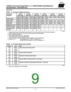
Erase operation. See Table 4 for software command
codes, Figure 16 for timing waveform and Figure 23 for a
flowchart.
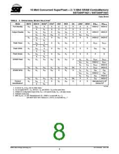
SRAM Read
The SRAM Read operation of the SST34HF1621/1641 is
controlled by OE# and BES1#, both have to be low with
WE# and BES2 high for the system to obtain data from the
outputs. BES1# and BES2 are used for SRAM bank selec-
tion. OE# is the output control and is used to gate data from
the output pins. The data bus is in high impedance state
when OE# is high. Refer to the Read cycle timing diagram,
Figure 3, for further details.
SRAM Operation
SRAM Write
With BES1# low, BES2 and BEF# high, the
SST34HF162x operates as 256K x8 or 128K x16 CMOS
SRAM, and the SST34HF164x operates as 512K x8 or
256K x16 CMOS SRAM, with fully static operation requir-
ing no external clocks or timing strobes. The CIOs pin
configures the SRAM for x8 or x16 SRAM operation
modes. The SST34HF162x SRAM is mapped into the
first 256 KByte/128 KWord address space of the device,
and the SST34HF164x SRAM is mapped into the first
512 KByte/256 KWord address space. When BES1#,
BEF# are high and BES2 is low, all memory banks are
The SRAM Write operation of the SST34HF1621/1641 is
controlled by WE# and BES1#, both have to be low, BES2
have to be high for the system to write to the SRAM. During
the Word-Write operation, the addresses and data are ref-
erenced to the rising edge of either BES1#, WE#, or the
falling edge of BES2 whichever occurs first. The write time
is measured from the last falling edge of BES#1 or WE# or
the rising edge of BES2 to the first rising edge of BES1#, or
WE# or the falling edge of BES2. Refer to the Write cycle
timing diagram, Figures 4 and 5, for further details.
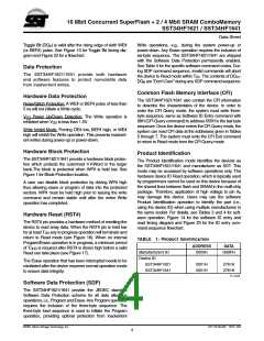
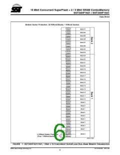
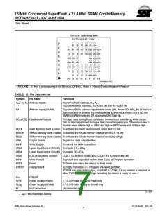
FUNCTIONAL BLOCK DIAGRAM
Address
Buffers
A
- A
0
MS
SuperFlash Memory
(Bank 1)
RST#
BEF#
WP#
SA
SuperFlash Memory
(Bank 2)
LBS#
UBS#
Control
Logic
WE#
OE#
DQ - DQ
15
8
I/O Buffers
BES1#
BES2
DQ - DQ
7
0
CIOs
RY/BY#
2 Mbit or 4 Mbit
SRAM
Address
Buffers
523 ILL B1.1
A
= Most significant address
MS
©2001 Silicon Storage Technology, Inc.
S71172-05-000 10/01 523
5

 SST [ SILICON STORAGE TECHNOLOGY, INC ]