16 Mbit Concurrent SuperFlash + 2 / 4 Mbit SRAM ComboMemory
SST34HF1621 / SST34HF1641
Data Sheet
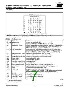
The flash and SRAM operate as two independent memory
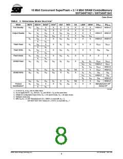
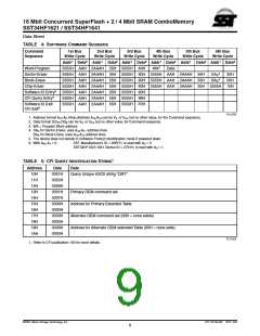
CONCURRENT READ/WRITE STATE TABLE
Flash
banks with respective bank enable signals. The memory
bank selection is done by two bank enable signals. The
SRAM bank enable signal, BES1# and BES2, selects the
SRAM bank. The flash memory bank enable signal, BEF#,
has to be used with Software Data Protection (SDP) com-
mand sequence when controlling the Erase and Program
operations in the flash memory bank. The memory banks
are superimposed in the same memory address space
where they share common address lines, data lines, WE#
and OE# which minimize power consumption and area.
Bus contention is eliminated as the device will not recog-
nize both bank enables as being simultaneously active.
Bank 1
Read
Bank 2
Write
SRAM
No Operation
No Operation
Read
Write
Read
Write
No Operation
Write
No Operation
Write
Read
No Operation
Write
Write
No Operation
Write
Note: For the purposes of this table, write means to Block-, Sector,
or Chip-Erase, or Word-Program as applicable to the
appropriate bank.
Designed, manufactured, and tested for applications requir-
ing low power and small form factor, the SST34HF1621/
1641 are offered in both commercial and extended temper-
atures and a small footprint package to meet board space
constraint requirements.
Flash Read Operation
The Read operation of the SST34HF1621/1641 is
controlled by BEF# and OE#, both have to be low for
the system to obtain data from the outputs. BEF# is
used for device selection. When BEF# is high, the
chip is deselected and only standby power is con-
sumed. OE# is the output control and is used to gate
data from the output pins. The data bus is in high
impedance state when either BEF# or OE# is high.
Refer to the Read cycle timing diagram for further
details (Figure 6).
Device Operation
The SST34HF1621/1641 uses BES1#, BES2 and BEF# to
control operation of either the flash or the SRAM memory
bank. When BEF# is low, the flash bank is activated for
Read, Program or Erase operation. When BES1# is low,
and BES2 is high the SRAM is activated for Read and
Write operation. BEF# and BES1# cannot be at low level,
and BES2 cannot be at high level at the same time. If all
bank enable signals are asserted, bus contention will result
and the device may suffer permanent damage. All address,
data, and control lines are shared by flash and SRAM
memory banks which minimizes power consumption and
loading. The device goes into standby when BEF# and
BES1# bank enables are raised to VIHC (Logic High) or
when BEF# is high and BES2 is low.
Flash Word-Program Operation
The SST34HF1621/1641 are programmed on a word-by-
word basis. Before Program operations, the memory must
be erased first. The Program operation consists of three
steps. The first step is the three-byte load sequence for
Software Data Protection. The second step is to load word
address and word data. During the Word-Program opera-
tion, the addresses are latched on the falling edge of either
BEF# or WE#, whichever occurs last. The data is latched
on the rising edge of either BEF# or WE#, whichever
occurs first. The third step is the internal Program operation
which is initiated after the rising edge of the fourth WE# or
BEF#, whichever occurs first. The Program operation, once
initiated, will be completed typically within 10 µs. See Fig-
ures 7 and 8 for WE# and BEF# controlled Program opera-
tion timing diagrams and Figure 21 for flowcharts. During
the Program operation, the only valid reads are Data# Poll-
ing and Toggle Bit. During the internal Program operation,
the host is free to perform additional tasks. Any commands
issued during the internal Program operation are ignored.
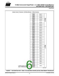
Concurrent Read/Write Operation
Dual bank architecture of SST34HF1621/1641 devices
allows the Concurrent Read/Write operation whereby the
user can read from one bank while program or erase in the
other bank. This operation can be used when the user
needs to read system code in one bank while updating
data in the other bank. See Figure 1 for Dual-Bank Memory
Organization.
©2001 Silicon Storage Technology, Inc.
S71172-05-000 10/01 523
2

 SST [ SILICON STORAGE TECHNOLOGY, INC ]