16 Mbit Concurrent SuperFlash + 2 / 4 Mbit SRAM ComboMemory
SST34HF1621 / SST34HF1641
Data Sheet
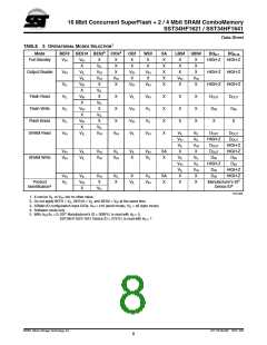
Toggle Bit (DQ6) is valid after the rising edge of sixth WE#
(or BEF#) pulse. See Figure 10 for Toggle Bit timing dia-
gram and Figure 22 for a flowchart.
Write operations, e.g., during the system power-up or
power-down. Any Erase operation requires the inclusion of
six-byte sequence. The SST34HF1621/1641 are shipped
with the Software Data Protection permanently enabled.
See Table 4 for the specific software command codes. Dur-
ing SDP command sequence, invalid commands will abort
the device to Read mode within TRC. The contents of DQ15-
DQ8 are “Don’t Care” during any SDP command sequence.
Data Protection
The SST34HF1621/1641 provide both hardware
and software features to protect nonvolatile data
from inadvertent writes.
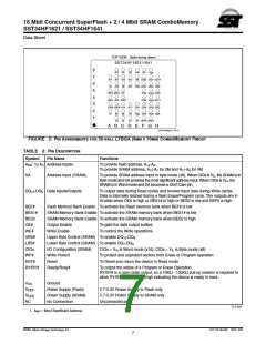
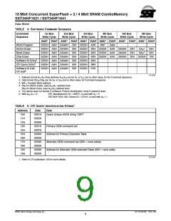
Common Flash Memory Interface (CFI)
Hardware Data Protection
The SST34HF1621/1641 also contain the CFI information
to describe the characteristics of the device. In order to
enter the CFI Query mode, the system must write three-
byte sequence, same as Software ID Entry command with
98H (CFI Query command) to address 555H in the last byte
sequence. Once the device enters the CFI Query mode, the
system can read CFI data at the addresses given in Tables
5 through 7. The system must write the CFI Exit command
to return to Read mode from the CFI Query mode.
Noise/Glitch Protection: A WE# or BEF# pulse of less than
5 ns will not initiate a Write cycle.
VDD Power Up/Down Detection: The Write operation is
inhibited when VDD is less than 1.5V.
Write Inhibit Mode: Forcing OE# low, BEF# high, or WE#
high will inhibit the Write operation. This prevents inadvert-
ent writes during power-up or power-down.
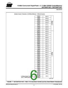
Hardware Block Protection
Product Identification
The SST34HF1621/1641 provide a hardware block protec-
tion which protects the outermost 4 KWord in the larger
bank.The block is protected when WP# is held low. See
Figure 1 for Block-Protection location.
The Product Identification mode identifies the devices as
the SST34HF1621/1641 and manufacturer as SST. This
mode may be accessed by software operations only. The
hardware device ID Read operation, which is typically used
by programmers cannot be used on this device because of
the shared lines between flash and SRAM in the multi-chip
package. Therefore, application of high voltage to pin A9
may damage this device. Users may use the software
Product Identification operation to identify the part (i.e.,
using the device ID) when using multiple manufacturers in
the same socket. For details, see Tables 3 and 4 for soft-
ware operation, Figure 14 for the software ID entry and
read timing diagram and Figure 23 for the ID entry com-
mand sequence flowchart.
A user can disable block protection by driving WP# high
thus allowing erase or program of data into the protected
sectors. WP# must be held high prior to issuing the write
command and remain stable until after the entire Write
operation has completed.
Hardware Reset (RST#)
The RST# pin provides a hardware method of resetting the
device to read array data. When the RST# pin is held low
for at least TRP, any in-progress operation will terminate and
return to Read mode (see Figure 18). When no internal
Program/Erase operation is in progress, a minimum period
of TRHR is required after RST# is driven high before a valid
Read can take place (see Figure 17).
TABLE 1: PRODUCT IDENTIFICATION
ADDRESS
DATA
Manufacturer’s ID
Device ID
0000H
00BFH
The Erase operation that has been interrupted needs to be
reinitiated after the device resumes normal operation mode
to ensure data integrity.
SST34HF1621
SST34HF1641
0001H
0001H
2761H
2761H
T1.2 523
Software Data Protection (SDP)
The SST34HF1621/1641 provide the JEDEC standard
Software Data Protection scheme for all data alteration
operations, i.e., Program and Erase. Any Program operation
requires the inclusion of the three-byte sequence. The
three-byte load sequence is used to initiate the Program
operation, providing optimal protection from inadvertent
©2001 Silicon Storage Technology, Inc.
S71172-05-000 10/01 523
4

 SST [ SILICON STORAGE TECHNOLOGY, INC ]