16 Mbit Concurrent SuperFlash + 2 / 4 Mbit SRAM ComboMemory
SST34HF1621 / SST34HF1641
Data Sheet
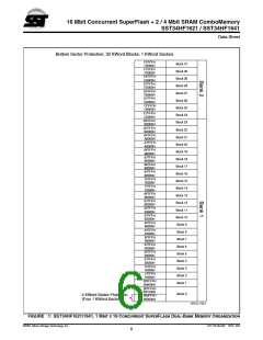
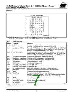
TOP VIEW (balls facing down)
SST34HF1621/1641
8
A15 NC
NC
A16 NC
SA DQ15 DQ7 DQ14
A10 DQ6 DQ13 DQ12 DQ5
V
SS
7
6
5
4
3
2
1
A11 A12 A13 A14
A8 A19 A9
WE# BES2 NC
WP# RST# RY/BY#
DQ4
DQ3
V
V
CIOs
DDS
DQ11
DDF
LBS# UBS# A18 A17 DQ1 DQ9 DQ10 DQ2
A7
A6
A3
A5
A2
A4
A1
V
OE# DQ0 DQ8
SS
A0 BEF# BES1#
A B C D E F G H
523 56-lfbga ILL P01.2
FIGURE 2: PIN ASSIGNMENTS FOR 56-BALL LFBGA (8MM X 10MM) COMBOMEMORY PINOUT
TABLE 2: PIN DESCRIPTION
Symbol
Pin Name
Functions
AMS1 to A0 Address Inputs
To provide flash address, A19-A0.
To provide SRAM address, A16-A0 for 2M and A17-A0 for 4M
SA
Address Input (SRAM)
To provide SRAM address input in byte mode (x8). When CIOs is VIL, the SRAM is in
Byte mode and SA provides the most significant address input. When CIOs is VIH, the
SRAM is in Word mode and SA becomes a Don’t Care pin.
DQ15-DQ0 Data Inputs/Outputs
To output data during Read cycles and receive input data during Write cycles.
Data is internally latched during a flash Erase/Program cycle. The outputs are in
tri-state when OE# is high or BES1# is high or BES2 is low and BEF# is high.
BEF#
BES1#
BES2
OE#
Flash Memory Bank Enable To activate the Flash memory bank when BEF# is low
SRAM Memory Bank Enable To activate the SRAM memory bank when BES1# is low
SRAM Memory Bank Enable To activate the SRAM memory bank when BES2 is high
Output Enable
Write Enable
To gate the data output buffers
To control the Write operations
WE#
UBS#
LBS#
CIOs
Upper Byte Control (SRAM) To enable DQ15-DQ8
Lower Byte Control (SRAM) To enable DQ7-DQ0
I/O Configuration (SRAM)
Write Protect
CIOs = VIH is Word mode (x16), CIOs = VIL is Byte mode (x8)
WP#
To protect and unprotect sectors from Erase or Program operation
To Reset and return the device to Read mode
RST#
RY/BY#
Reset
Ready/Busy#
To output the status of a Program or Erase Operation
RY/BY# is a open drain output, so a 10KΩ - 100KΩ pull-up resistor is required to
allow RY/BY# to transition high indicating the device is ready to read.
VSS
Ground
VDDF
Power Supply (Flash)
Power Supply (SRAM)
No Connection
2.7-3.3V Power Supply to Flash only
2.7-3.3V Power Supply to SRAM only
Unconnected pins
VDD
S
NC
T2.5 523
1. AMS = Most Significant Address
©2001 Silicon Storage Technology, Inc.
S71172-05-000 10/01 523
7

 SST [ SILICON STORAGE TECHNOLOGY, INC ]