16 Mbit Concurrent SuperFlash + 2 / 4 Mbit SRAM ComboMemory
SST34HF1621 / SST34HF1641
Data Sheet
i.e., valid data may appear to conflict with either DQ7 or
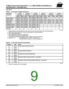
Flash Sector/Block-Erase Operation
DQ6. In order to prevent spurious rejection, if an erroneous
result occurs, the software routine should include a loop to
read the accessed location an additional two (2) times. If
both reads are valid, then the device has completed the
Write cycle, otherwise the rejection is valid.
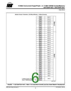
The Sector/Block-Erase operation allows the system to
erase the device on a sector-by-sector or block-by-block
basis. The SST34HF1621/1641 offer both Sector-Erase
and Block-Erase mode. The sector architecture is based
on uniform sector size of 1 KWord. The Block-Erase mode
is based on uniform block size of 32 KWord. The Sector-
Erase operation is initiated by executing a six-byte com-
mand sequence with Sector-Erase command (30H) and
sector address (SA) in the last bus cycle. The Block-Erase
operation is initiated by executing a six-byte command
sequence with Block-Erase command (50H) and block
address (BA) in the last bus cycle. The sector or block
address is latched on the falling edge of the sixth WE#
pulse, while the command (30H or 50H) is latched on the
rising edge of the sixth WE# pulse. The internal Erase
operation begins after the sixth WE# pulse. See Figures 12
and 13 for timing waveforms. Any commands issued during
the Sector- or Block-Erase operation are ignored.
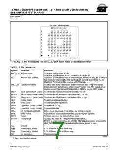
Ready/Busy# (RY/BY#)
The SST34HF1621/1641 includes a Ready/Busy# (RY/
BY#) output signal. RY/BY# is actively pulled low during
internal Program/Erase operation. The status of RY/BY# is
valid after the rising edge of fourth WE# (or CE#) pulse for
Program operation. For Sector-, Block- or Bank-Erase, the
RY/BY# is valid after the rising edge of sixth WE# or (CE#)
pulse. RY/BY# is an open drain output that allows several
devices to be tied in parallel to VDD via an external pull up
resistor. Ready/Busy# is in high impedance whenever OE#
or CE# is high or RST# is low.
Flash Data# Polling (DQ7)
Flash Chip-Erase Operation
When the SST34HF1621/1641 are in the internal Program
operation, any attempt to read DQ7 will produce the com-
plement of the true data. Once the Program operation is
completed, DQ7 will produce true data. Note that even
though DQ7 may have valid data immediately following the
completion of an internal Write operation, the remaining
data outputs may still be invalid: valid data on the entire
data bus will appear in subsequent successive Read
cycles after an interval of 1 µs. During internal Erase opera-
tion, any attempt to read DQ7 will produce a ‘0’. Once the
internal Erase operation is completed, DQ7 will produce a
‘1’. The Data# Polling (DQ7) is valid after the rising edge of
fourth WE# (or BEF#) pulse for Program operation. For
Sector-, Block- or Chip-Erase, the Data# Polling (DQ7) is
valid after the rising edge of sixth WE# (or BEF#) pulse.
After the completion of a Program operation, Data# Polling
on DQ7 remains active and the device may not return to the
Read mode for approximately 1 µs. See Figure 9 for Data#
Polling (DQ7) timing diagram and Figure 22 for a flowchart.
The SST34HF1621/1641 provide a Chip-Erase operation,
which allows the user to erase all unprotected sectors/
blocks to the “1” state. This is useful when the device must
be quickly erased.
The Chip-Erase operation is initiated by executing a six-
byte command sequence with Chip-Erase command (10H)
at address 5555H in the last byte sequence. The Erase
operation begins with the rising edge of the sixth WE# or
BEF#, whichever occurs first. During the Erase operation,
the only valid read is Toggle Bit or Data# Polling. See Table
4 for the command sequence, Figure 11 for timing diagram,
and Figure 24 for the flowchart. Any commands issued dur-
ing the Chip-Erase operation are ignored.
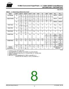
Flash Write Operation Status Detection
The SST34HF1621/1641 provide one hardware and two
software means to detect the completion of a Write (Pro-
gram or Erase) cycle, in order to optimize the system
Write cycle time. The hardware detection uses the
Ready/Busy# (RY/BY#) pin. The software detection
includes two status bits: Data# Polling (DQ7) and Toggle
Bit (DQ6). The End-of-Write detection mode is enabled
after the rising edge of WE#, which initiates the internal
Program or Erase operation.
Flash Toggle Bit (DQ6)
During the internal Program or Erase operation, any con-
secutive attempts to read DQ6 will produce alternating 1s
and 0s, i.e., toggling between 1 and 0. When the internal
Program or Erase operation is completed, the DQ6 bit will
stop toggling. After the completion of a Program operation,
DQ6 will stop toggling for approximately 1 µs. The device is
then ready for the next operation. The Toggle Bit (DQ6) is
valid after the rising edge of fourth WE# (or BEF#) pulse for
Program operation. For Sector-, Block- or Chip-Erase, the
The actual completion of the nonvolatile write is asynchro-
nous with the system; therefore, either a Ready/Busy# (RY/
BY#), Data# Polling (DQ7) or Toggle Bit (DQ6) read may be
simultaneous with the completion of the Write cycle. If this
occurs, the system may possibly get an erroneous result,
©2001 Silicon Storage Technology, Inc.
S71172-05-000 10/01 523
3

 SST [ SILICON STORAGE TECHNOLOGY, INC ]