A d v a n c e I n f o r m a t i o n
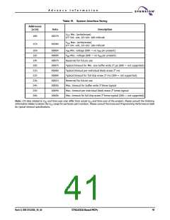
Table 19. System Interface String
Addresses
(x16)
Data
Description
VCC Min. (write/erase)
D7–D4: volt, D3–D0: 100 millivolt
1Bh
1Ch
0027h
VCC Max. (write/erase)
D7–D4: volt, D3–D0: 100 millivolt
0036h
1Dh
1Eh
1Fh
20h
21h
22h
23h
24h
25h
26h
0000h
0000h
0007h
0007h
000Ah
0000h
0001h
0005h
0004h
0000h
VPP Min. voltage (00h = no VPP pin present)
VPP Max. voltage (00h = no VPP pin present)
Reserved for future use
Typical timeout for Min. size buffer write 2N
µs (00h = not supported)
Typical timeout per individual block erase 2N ms
Typical timeout for full chip erase 2N ms (00h = not supported)
Reserved for future use
Max. timeout for buffer write 2N times typical
Max. timeout per individual block erase 2N times typical
Max. timeout for full chip erase 2N times typical (00h = not supported)
Note: CFI data related to V and time-outs may differ from actual V and time-outs of the product. Please consult the Ordering
CC
CC
Information tables to obtain the V range for particular part numbers. Please consult the Erase and Programming Performance table
CC
for typical timeout specifications.
March 31, 2005 S71GL032A_00_A0
S71GL032A Based MCPs
41

 SPANSION [ SPANSION ]