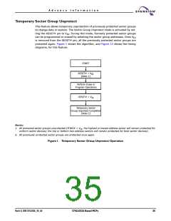
A d v a n c e I n f o r m a t i o n
Low V
Write Inhibit
CC
When VCC is less than VLKO, the device does not accept any write cycles. This pro-
tects data during VCC power-up and power-down. The command register and all
internal program/erase circuits are disabled, and the device resets to the read
mode. Subsequent writes are ignored until VCC is greater than VLKO. The system
must provide the proper signals to the control pins to prevent unintentional writes
when VCC is greater than VLKO
.
Write Pulse “Glitch” Protection
Noise pulses of less than 3 ns (typical) on OE#, CE# or WE# do not initiate a write
cycle.
Logical Inhibit
Write cycles are inhibited by holding any one of OE# = VIL, CE# = VIH or WE# =
VIH. To initiate a write cycle, CE# and WE# must be a logical zero while OE# is a
logical one.
Power-Up Write Inhibit
If WE# = CE# = VIL and OE# = VIH during power up, the device does not accept
commands on the rising edge of WE#. The internal state machine is automatically
reset to the read mode on power-up.
March 31, 2005 S71GL032A_00_A0
S71GL032A Based MCPs
39

 SPANSION [ SPANSION ]