A d v a n c e I n f o r m a t i o n
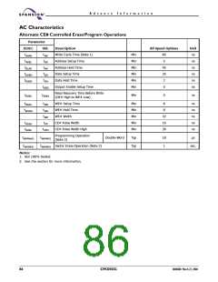
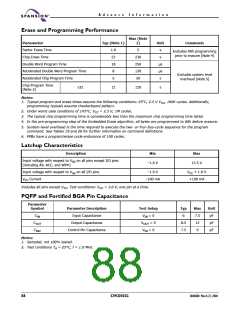
Erase and Programming Performance
Max (Note
2)
Parameter
Typ (Note 1)
Unit
s
Comments
Sector Erase Time
1.0
23
18
8
5
Excludes 00h programming
prior to erasure (Note 4)
Chip Erase Time
230
250
130
50
s
Double Word Program Time
Accelerated Double Word Program Time
Accelerated Chip Program Time
µs
µs
s
Excludes system level
overhead (Note 5)
5
Chip Program Time
x32
12
120
s
(Note 3)
Notes:
1. Typical program and erase times assume the following conditions: 25°C, 2.5 V VCC, 100K cycles. Additionally,
programming typicals assume checkerboard pattern.
2. Under worst case conditions of 145°C, VCC = 2.5 V, 1M cycles.
3. The typical chip programming time is considerably less than the maximum chip programming time listed.
4. In the pre-programming step of the Embedded Erase algorithm, all bytes are programmed to 00h before erasure.
5. System-level overhead is the time required to execute the two- or four-bus-cycle sequence for the program
command. See Tables 19 and 20 for further information on command definitions.
6. PPBs have a program/erase cycle endurance of 100 cycles.
Latchup Characteristics
Description
Min
Max
Input voltage with respect to V on all pins except I/O pins
SS
(including A9, ACC, and WP#)
–1.0 V
12.5 V
Input voltage with respect to V on all I/O pins
–1.0 V
V
+ 1.0 V
SS
CC
V
Current
–100 mA
+100 mA
CC
Includes all pins except VCC. Test conditions: VCC = 3.0 V, one pin at a time.
PQFP and Fortified BGA Pin Capacitance
Parameter
Symbol
Parameter Description
Input Capacitance
Test Setup
Typ
6
Max
7.5
12
Unit
pF
C
V
= 0
= 0
= 0
IN
IN
C
Output Capacitance
V
8.5
7.5
pF
OUT
OUT
C
Control Pin Capacitance
V
9
pF
IN2
IN
Notes:
1. Sampled, not 100% tested.
2. Test conditions TA = 25°C, f = 1.0 MHz.
88
S29CD032G
30606B0 March 22, 2004

 SPANSION [ SPANSION ]