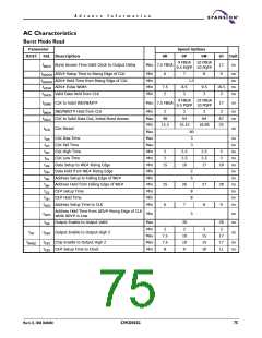
A d v a n c e I n f o r m a t i o n
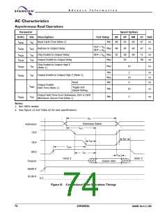
AC Characteristics
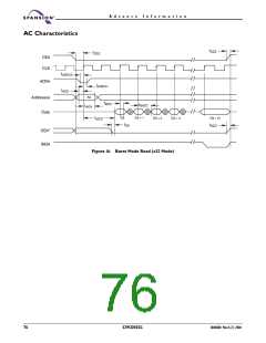
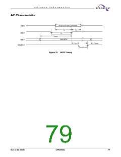
Burst Mode Read
Parameter
Speed Options
JEDEC
Std. Description
0R
0P
0M
10 FBGA
0J
17
9
Unit
9 FBGA
9.5 PQFP 10 PQFP
t
Burst Access Time Valid Clock to Output Delay
Max 7.5 FBGA
ns
BACC
t
ADV# Setup Time to Rising Edge of CLK
ADV# Hold Time from Rising Edge of CLK
ADV# Pulse Width
Min
Min
Min
Min
6
7
8
ns
ns
ns
ns
ADVCS
t
1.5
ADVCH
t
7.5
2
8.5
2
9.5
3
10.5
3
ADVP
t
Valid Data Hold from CLK
DVCH
9 FBGA
9.5 PQFP 10 PQFP
10 FBGA
t
t
CLK to Valid IND/WAIT#
Max 7.5 FBGA
17
ns
DIND
IND/WAIT# Hold from CLK
Min
Max
Min
Max
Max
Max
Min
Min
Min
Min
Min
Min
Min
Min
Min
2
2
3
3
ns
ns
INDH
t
CLK to Valid Data Out, Initial Burst Access
48
54
64
67
25
IACC
13.3
15.15
18.85
t
CLK Period
ns
CLK
60
3
t
CLK Rise Time
ns
ns
ns
ns
ns
ns
ns
ns
ns
ns
ns
CR
t
CLK Fall Time
3
CF
t
CLK High Time
2
2
2.5
2.5
16
2.5
2.5
17
3
3
CH
t
CLK Low Time
CL
DS
DH
t
Data Setup to WE# Rising Edge
Data Hold from WE# Rising Edge
Address Setup to Falling Edge of WE#
Address Hold from Falling Edge of WE#
CE# Setup Time
15
18
t
2
5
t
AS
AH
t
25
6
26
7
27
8
28
9
t
8
8
CS
CH
t
CE# Hold Time
t
Address Setup Time to CLK
ACS
Address Hold Time from ADV# Rising Edge of CLK
while ADV# is Low
t
Min
3
ns
ns
ACH
t
Output Enable to Output Valid
Max
Min
Max
Max
Min
20
2
28
3
OE
2
3
t
t
Output Enable to Output High Z
ns
DF
OEZ
7.5
7.5
8
10
10
9
15
15
10
17
17
11
t
t
t
Chip Enable to Output High Z
CE# Setup Time to Clock
ns
ns
EHQZ
CEZ
CES
March 22, 2004 30606B0
S29CD032G
75

 SPANSION [ SPANSION ]