4th Generation USB2.0 Flash Media Controller with Integrated Card Power FETs and HS Hub
Datasheet
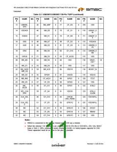
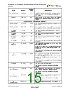
BUFFER
NAME
SYMBOL
TYPE
DESCRIPTION
Over Current Sense
OCS[4:2]_N
IPU
Input from external current monitor indicating an over-
current condition. {Note: Contains internal pull-up to
3.3V supply}
Green LED
GR[4:2]_N
I/O8
Green indicator LED for ports 2, 3 and 4. Will be active
low when LED support is enabled via EEPROM or
SMBus.
CompactFlash (In True IDE mode) INTERFACE
CF Chip Select 1
CF Chip Select 0
CF_nCS1
O8PU
O8PU
O8
This pin is the active low chip select 1 signal for the CF
ATA device
CF_nCS0
CF_SA2
CF_SA1
CF_SA0
CF_IRQ
This pin is the active low chip select 0 signal for the task
file registers of CF ATA device in the True IDE mode.
CF Register
Address 2
This pin is the register select address bit 2 for the CF
ATA device.
CF Register
Address 1
O8
This pin is the register select address bit 1 for the CF
ATA device
CF Register
Address 0
O8
This pin is the register select address bit 0 for the CF
ATA device.
CF Interrupt
IPD
This is the active high interrupt request signal from the
CF device.
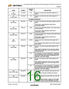
CF
CF_D[15:8]
I/O8PD
The bi-directional data signals CF_D15-CF_D8 in True
IDE mode data transfer.
Data 15-8
In the True IDE Mode, all of task file register operation
occur on the CF_D[7:0], while the data transfer is on
CF_D[15:0].
The bi-directional data signal has an internal weak pull-
down resistor.
CF
CF_D[7:0]
I/O8PD
The bi-directional data signals CF_D7-CF_D0 in the
True IDE mode data transfer.
Data7-0
In the True IDE Mode, all of task file register operation
occur on the CF_D[7:0], while the data transfer is on
CF_D[15:0].
The bi-directional data signal has an internal weak pull-
down resistor.
IO Ready
CF_IORDY
CF_nCD2
IPU
IPU
This pin is active high input signal.
This pin has an internally controlled weak pull-up
resistor.
CF
This card detection pin is connected to the ground on
the CF device, when the CF device is inserted.
Card Detection2
This pin has an internally controlled weak pull-up
resistor.
CF
CF_nCD1
IPU
O8
This card detection pin is connected to ground on the
CF device, when the CF device is inserted.
Card Detection1
This pin has an internally controlled weak pull-up
resistor.
CF
CF_nRESET
This pin is an active low hardware reset signal to CF
device.
Hardware Reset
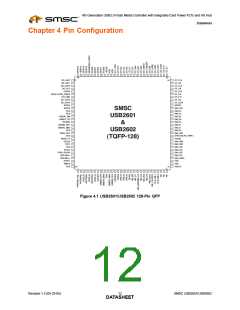
SMSC USB2601/USB2602
Revision 1.3 (05-25-05)
DATA1S5HEET

 SMSC [ SMSC CORPORATION ]