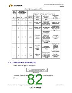
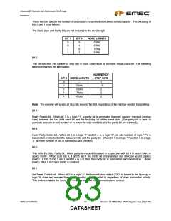
Advanced I/O Controller with Motherboard GLUE Logic
Datasheet
Bit 5
Transmitter Holding Register Empty (THRE). Bit 5 indicates that the Serial Port is ready to accept a new
character for transmission. In addition, this bit causes the Serial Port to issue an interrupt when the
Transmitter Holding Register interrupt enable is set high. The THRE bit is set to a logic “1” when a
character is transferred from the Transmitter Holding Register into the Transmitter Shift Register. The bit is
reset to logic “0” whenever the CPU loads the Transmitter Holding Register. In the FIFO mode this bit is
set when the XMIT FIFO is empty, it is cleared when at least 1 byte is written to the XMIT FIFO. Bit 5 is a
read only bit.
Bit 6
Transmitter Empty (TEMT). Bit 6 is set to a logic “1” whenever the Transmitter Holding Register (THR)
and Transmitter Shift Register (TSR) are both empty. It is reset to logic “0” whenever either the THR or
TSR contains a data character. Bit 6 is a read only bit. In the FIFO mode this bit is set whenever the
THR and TSR are both empty,
Bit 7
This bit is permanently set to logic “0” in the 450 mode. In the FIFO mode, this bit is set to a logic “1” when
there is at least one parity error, framing error or break indication in the FIFO. This bit is cleared when the
LSR is read if there are no subsequent errors in the FIFO.
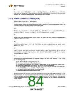
6.28.10 MODEM STATUS REGISTER (MSR)
Address Offset = 6H, DLAB = X, READ/WRITE
This 8 bit register provides the current state of the control lines from the MODEM (or peripheral device). In
addition to this current state information, four bits of the MODEM Status Register (MSR) provide change
information. These bits are set to logic “1” whenever a control input from the MODEM changes state. They
are reset to logic “0” whenever the MODEM Status Register is read.
Bit 0
Delta Clear To Send (DCTS). Bit 0 indicates that the nCTS input to the chip has changed state since the
last time the MSR was read.
Bit 1
Delta Data Set Ready (DDSR). Bit 1 indicates that the nDSR input has changed state since the last time
the MSR was read.
Bit 2
Trailing Edge of Ring Indicator (TERI). Bit 2 indicates that the nRI input has changed from logic “0” to logic
“1”.
Bit 3
Delta Data Carrier Detect (DDCD). Bit 3 indicates that the nDCD input to the chip has changed state.
Note: Whenever bit 0, 1, 2, or 3 is set to a logic “1”, a MODEM Status Interrupt is generated.
Revision 1.8 SMSC/Non-SMSC Register Sets (02-24-05)
86
SMSC LPC47M182
DATASHEET

 SMSC [ SMSC CORPORATION ]