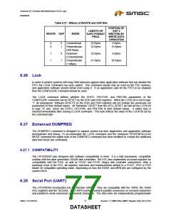
Advanced I/O Controller with Motherboard GLUE Logic
Datasheet
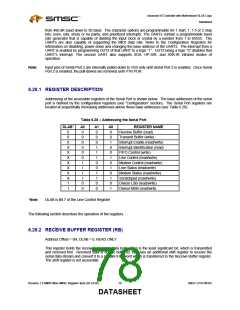
6.28.5 FIFO CONTROL REGISTER (FCR)
Address Offset = 2H, DLAB = X, WRITE
This is a write only register at the same location as the IIR. This register is used to enable and clear the
FIFOs, set the RCVR FIFO trigger level. Note: DMA is not supported. The UART is shadowed in the
UART1 FIFO Control Shadow Register (Located at offset 0x1A in the Power Control Logical Device, when
LD_NUM=0, or Runtime Register Block Logical Device, when LD_NUM=1).
Bit 0
Setting this bit to a logic “1” enables both the XMIT and RCVR FIFOs. Clearing this bit to a logic “0”
disables both the XMIT and RCVR FIFOs and clears all bytes from both FIFOs. When changing from FIFO
Mode to non-FIFO (16450) mode, data is automatically cleared from the FIFOs. This bit must be a 1 when
other bits in this register are written to or they will not be properly programmed.
Bit 1
Setting this bit to a logic “1” clears all bytes in the RCVR FIFO and resets its counter logic to 0. The shift
register is not cleared. This bit is self-clearing.
Bit 2
Setting this bit to a logic “1” clears all bytes in the XMIT FIFO and resets its counter logic to 0. The shift
register is not cleared. This bit is self-clearing.
Bit 3
Writing to this bit has no effect on the operation of the UART. The RXRDY and TXRDY pins are not
available on this chip.
Bit 4,5
Reserved
Bit 6,7
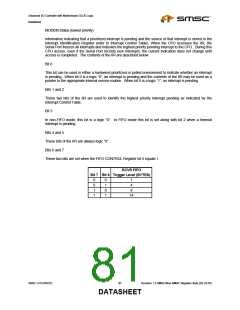
These bits are used to set the trigger level for the RCVR FIFO interrupt.
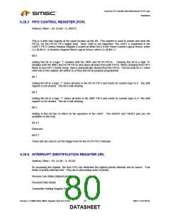
6.28.6 INTERRUPT IDENTIFICATION REGISTER (IIR)
Address Offset = 2H, DLAB = X, READ
By accessing this register, the host CPU can determine the highest priority interrupt and its source. Four
levels of priority interrupt exist. They are in descending order of priority:
Receiver Line Status (highest priority)
Received Data Ready
Transmitter Holding Register Empty
Revision 1.8 SMSC/Non-SMSC Register Sets (02-24-05)
80
SMSC LPC47M182
DATASHEET

 SMSC [ SMSC CORPORATION ]