Advanced I/O Controller with Motherboard GLUE Logic
Datasheet
from 460.8K baud down to 50 baud. The character options are programmable for 1 start; 1, 1.5 or 2 stop
bits; even, odd, sticky or no parity; and prioritized interrupts. The UARTs contain a programmable baud
rate generator that is capable of dividing the input clock or crystal by a number from 1 to 65535. The
UARTs are also capable of supporting the MIDI data rate. Refer to the Configuration Registers for
information on disabling, power down and changing the base address of the UARTs. The interrupt from a
UART is enabled by programming OUT2 of that UART to a logic “1”. OUT2 being a logic “0” disables that
UART’s interrupt. The second UART also supports IrDA, HP-SIR, and ASK-IR infrared modes of
operation.
Note:
Input pins of Serial Port 2 are internally pulled down to VSS only until Serial Port 2 is enabled. Once Serial
Port 2 is enabled, the pull-downs are removed until VTR POR.
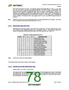
6.28.1 REGISTER DESCRIPTION
Addressing of the accessible registers of the Serial Port is shown below. The base addresses of the serial
port is defined by the configuration registers (see “Configuration” section). The Serial Port registers are
located at sequentially increasing addresses above these base addresses (see Table 6.28).
Table 6.28 – Addressing the Serial Port
DLAB*
A2
0
0
0
0
0
0
1
1
1
1
0
0
A1
0
0
0
1
1
1
0
0
1
1
0
0
A0
0
0
1
0
0
1
0
1
0
1
0
1
REGISTER NAME
Receive Buffer (read)
Transmit Buffer (write)
0
0
0
Interrupt Enable (read/write)
Interrupt Identification (read)
FIFO Control (write)
Line Control (read/write)
Modem Control (read/write)
Line Status (read/write)
Modem Status (read/write)
Scratchpad (read/write)
Divisor LSB (read/write)
Divisor MSB (read/write
X
X
X
X
X
X
X
1
1
*Note:
DLAB is Bit 7 of the Line Control Register
The following section describes the operation of the registers.
6.28.2 RECEIVE BUFFER REGISTER (RB)
Address Offset = 0H, DLAB = 0, READ ONLY
This register holds the received incoming data byte. Bit 0 is the least significant bit, which is transmitted
and received first. Received data is double buffered; this uses an additional shift register to receive the
serial data stream and convert it to a parallel 8 bit word which is transferred to the Receive Buffer register.
The shift register is not accessible.
Revision 1.8 SMSC/Non-SMSC Register Sets (02-24-05)
78
SMSC LPC47M182
DATASHEET

 SMSC [ SMSC CORPORATION ]