Advanced I/O Controller with Motherboard GLUE Logic
Datasheet
BUFFER
NAME
PWR
WELL
NAME
PIN#
DESCRIPTION
NOTES
(NOTE 1)
(NOTE 2)
(NOTE 3)
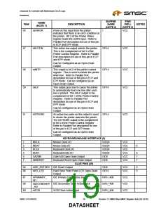
106,
108,
109
GP13-GP15
General Purpose I/O. GPIO can be
configured as an open-drain output.
IO8
VTR
6
111
GP16/
General Purpose I/O. GPIO can be
configured as an open-drain output.
IO8
IO8
VTR
6
6
Fan Tachometer 1 Input
FAN_TACH1
GP17/
112
General Purpose I/O. GPIO can be
VTR
VTR
configured as an open-drain output.
Fan Tachometer 2 Input
FAN_TACH2
TEST_EN
TEST (1)
98
Test Enable Input for XOR-Chain test –
the external pull-up or internal pull-down
sets the strap value. The XOR output is
the nDTR1 pin.
IPD
NO CONNECT (1)
117
NC
No Connect
IPD
-
11
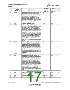
Note 1: The “n” as the first letter of a signal name or the “#” as the suffix of a signal name indicates an “Active Low”
signal. The primary and secondary functions on the pins are separated by “/”.
Note 2: The buffer names are described in the “Buffer Name Descriptions” section.
Note 3: Open-drain pins should be pulled-up externally to supply shown in the power well column. The
nIDE_RSTDRV, nHD_LED, DDCSDA_5V and DDCSCL_5V open-drain pins require external pull-ups to
VCC5V. The nBACKFEED_CUT, SCK_BJT_GATE and nPS_ON open-drain pins require external pull-
ups to V_5P0_STBY. Inputs with internal pull-ups are pulled internally to the supply shown in the power
well column. All other pins are driven under the power well shown. See the “Pins With Internal Resistors”,
“Pins That Require External Resistors” and “Default State of Pins” sections.
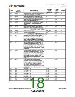
Note 4: The 32.768 kHz input clock must not be driven high when VTR = 0V. CLOCKI32 is clock source to various
logic in the part, including LED, “wake on specific key” and nFPRST debounce circuitry. The 32 KHz input
clock must always be connected. There is a bit in the configuration register at 0xF0 in Logical Device A
that indicates whether or not the 32KHz clock is connected. This bit determines the clock source for the
logic. This bit must always be set to ‘0’ (‘0’=32 KHz clock connected; reset default=‘0’).
Note 5: The nLPCPD pin may be tied high. The LPC interface will function properly if the nPCI_RESET signal
follows the protocol defined for the nLRESET signal in the “Low Pin Count Interface Specification”.
However, if nLPCPD is tied high, the keyboard wakeup isolation logic will be affected.
Note 6: These pins (except DDC and FAN_TACH functions) are also inputs to VTR powered logic internal to the
part. If DDC and FAN_TACH functions are selected on GPIOs, the pins will tri-state when VCC power is
removed.
Note 7: External pullups must be placed on the nKBDRST and GA20M pins. If the nKBDRST and GA20M
functions are to be used, the system must ensure that these pins are high. See the “That Require External
Resistors” section.
Note 8: When DDC functions are selected on GP20-GP23, the pins become IO_SW type and require external pull-
ups to the appropriate voltages. See the “That Require External Resistors” section. When the GPIO
functions are selected, the pins are IS0D8.
Note 9: The IRTX2 pin is driven low upon power-up of VCC. This pin will remain low following a power-up (VCC
POR) until it is selected via the IR MUX bits and serial port 2 is enabled by setting the activate bit, at which
SMSC LPC47M182
21
Revision 1.8 SMSC/Non-SMSC Register Sets (02-24-05)
DATASHEET

 SMSC [ SMSC CORPORATION ]