Advanced I/O Controller with Motherboard GLUE Logic
Datasheet
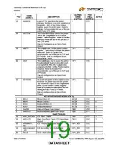
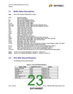
3.1
Buffer Name Descriptions
Note:
Refer to the “Electrical Characteristics” section.
PWR
I
Power and Ground
Input TTL Compatible.
IPU
Input with 30uA Integrated Pull-Up
IPD
Input with 30uA Integrated Pull-Down
IS
Input with 250mV Schmitt Trigger.
IS_400
ISPU_400
ISPD_400
O8
Input with 400mV Schmitt Trigger.
Input with 400mV Schmitt Trigger and 30uA Integrated Pull-Up.
Input with 400mV Schmitt Trigger and 30uA Integrated Pull-Down.
Output, 8mA sink, 4mA source.
OD8
Output (Open Drain), 8mA sink.
O12
Output, 12mA sink, 6mA source.
OD12
OP14
OD24
AO
Output (Open Drain), 12mA sink.
Output, 14mA sink, 14mA source.
Output (Open Drain), 24mA sink.
Output – Analog with 5V Level
IO8
Input/Output, 8mA sink, 4mA source.
ISO8
ISOD8
IO12
IOP14
IOD24
IO_SW
Input with 250mV Schmitt Trigger /Output, 8mA sink, 4mA source.
Input with 250mV Schmitt Trigger, Low Leakage/Output (Open-Drain), 8mA sink.
Input with Schmitt Trigger/Output, 12mA sink, 6mA source.
Input/Output, 14mA sink, 14mA source.
Input/Output (Open Drain), 24mA sink.
Input/Output, special type. Pins of this type are connected in pairs through a switch. The switch
provides a 25 ohm (max) resistance to ground when closed.
Input/Output. These pins meet the PCI 3.3V AC and DC Characteristics. (Note 1)
Output. These pins meet the PCI 3.3V AC and DC Characteristics. (Note 1)
Input. These pins meet the PCI 3.3V AC and DC Characteristics. (Note 1)
Clock Input. These pins meet the PCI 3.3V AC and DC Characteristics and timing. (Note 2)
PCI_IO
PCI_O
PCI_I
PCI_ICLK
Note 1:
Note 2:
See the “PCI Local Bus Specification,” Revision 2.1, Section 4.2.2.
See the “PCI Local Bus Specification,” Revision 2.1, Section 4.2.2 and 4.2.3.
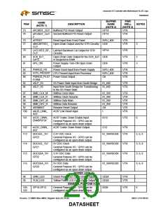
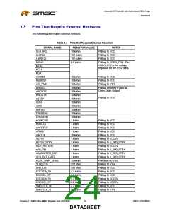
3.2
Pins With Internal Resistors
The following pins have internal resistors:
Table 3.2 – Pins with Internal Resistors
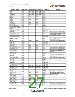
SIGNAL NAME
nCPU_PRESENT
nFPRST
nPRIMARY_HD
PWRGD_PS
nSCSI
nSECONDARY_HD
TEST_EN
RESISTOR VALUE
30uA
NOTES
Pull-up to VTR
30uA
30uA
30uA
30uA
30uA
30uA
Pull-up to VTR
Pull-up to VCC
Pull-up to VTR
Pull-up to VCC
Pull-up to VCC
Pull-down to VSS
SMSC LPC47M182
23
Revision 1.8 SMSC/Non-SMSC Register Sets (02-24-05)
DATASHEET

 SMSC [ SMSC CORPORATION ]