Advanced I/O Controller with Motherboard GLUE Logic
Datasheet
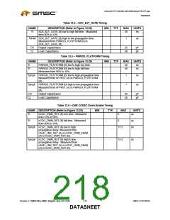
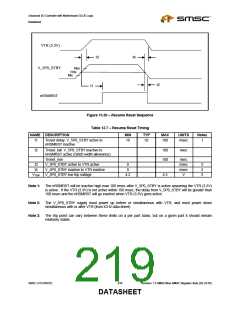
VTR (3.3V)
t3
t4
V_5P0_STBY
nRSMRST
Max
Vtrip
Min
t2
t1
Figure 13.30 – Resume Reset Sequence
Table 13.7 – Resume Reset Timing
NAME DESCRIPTION
MIN
10
TYP
32
MAX
100
UNITS
msec
Notes
t1
Treset delay. V_5P0_STBY active to
1
nRSMRST inactive
t2
Treset_fall. V_5P0_STBY inactive to
100
100
nsec
nRSMRST active (Glitch width allowance)
Treset_rise
V_5P0_STBY active to VTR active
V_5P0_STBY inactive to VTR inactive
nsec
msec
msec
V
t3
t4
0
0
4.2
2
2
3
VTRIP V_5P0_STBY low trip voltage
4.5
Note 1: The nRSMRST will be inactive high max 100 msec after V_5P0_STBY is active assuming the VTR (3.3V)
is active. If the VTR (3.3V) is not active within 100 msec, the delay from V_5P0_STBY will be greater than
100 msec and the nRSMRST will go inactive when VTR (3.3V) goes active.
Note 2: The V_5P0_STBY supply must power up before or simultaneous with VTR, and must power down
simultaneous with or after VTR (from ICH2 data sheet)
Note 3: The trip point can vary between these limits on a per part basis, but on a given part it should remain
relatively stable.
SMSC LPC47M182
219
Revision 1.8 SMSC/Non-SMSC Register Sets (02-24-05)
DATASHEET

 SMSC [ SMSC CORPORATION ]