Advanced I/O Controller with Motherboard GLUE Logic
Datasheet
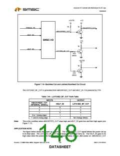
7.40 Resume Reset Logic
Table 7.47 – nRSMRST Pin
POWER
NAME
BUFFER
DESCRIPTION
WELL
VTR
nRSMRST
V_5P0_STBY
O8
Resume Reset Output
5V Standby
PWR
The nRSMRST signal is the reset output for the ICH resume well. This signal is used as a power on reset
signal as well as a brown-out sensor for the ICH.
The rising edge of nRSMRST is a delayed 3.3V buffered copy of V_5P0_STBY. This delay, tRESET_DELAY
,
nominally 32ms, starts when V_5P0_STBY hits the trip point, VTRIP. Note the nRSMRST will be inactive
high after the tRESET_DELAY only if VTR (3.3V) is present. Otherwise, nRSMRST will be active low beyond
the t
– until VTR (3.3V) goes active. On the falling edge there is minimal delay, tRESET_FALL. Note
RESET_DELAY
that VTRIP shown in Figure 26 has a VTRIP_MIN and a VTRIP_MAX. See Table below for timing and voltage
parameters.
Note that no internal clock is available during nRSMRST generation, so an internally generated delay is
required. The requirements are loose enough that an onboard RC delay is permissible. This delay is only
required at V_5P0_STBY power on and brown-out recovery.
See Table 13.7 for nRSMRST timing.
7.41 CNR Logic
Table 7.48 – CNR Pins
POWER
NAME
TYPE
DESCRIPTION
WELL
VTR
nAUD_LNK_RST
I
Audio Link Reset Input
nCDC_DWN_ENAB/
IO12
VTR
CODEC Down Enable
GP24
Input/GPIO
nCDC_DWN_RST
O12
VTR
CODEC Down Reset Output
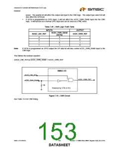
The CNR CODEC Down Enable Circuitry is used in conjunction with soft audio and motherboards with a
CNR slot. This feature allows the Basic Input / Output System (BIOS) to enable an audio CNR board. See
figure and table below for implementation and definition of the input and output states. Note that these
signals are required in all sleep states. The CNR circuitry is powered from VTR.
The nCDC_DWN_ENAB pin also functions as a GPIO. This allows BIOS to drive the pin to a known state
if the motherboard requires it. Note that nCDC_DWN_RST still follows the nCDC_DWN_ENAB pin even
when it is functioning as a GPIO output.
The nCDC_DWN_ENAB/GP24 pin functions as follows:
When the nCDC_DWN_ENAB function is selected on GP24, it will be an input to the CNR logic. The
polarity bit will not affect the input.
If GP24 is programmed as GPIO output the GP data bit will control nCDC_DWN_ENAB input to the
CNR logic. The data bit will also be reflected on the GP24 pin as an output under both VCC and VTR
Revision 1.8 SMSC/Non-SMSC Register Sets (02-24-05)
152
SMSC LPC47M182
DATASHEET

 SMSC [ SMSC CORPORATION ]