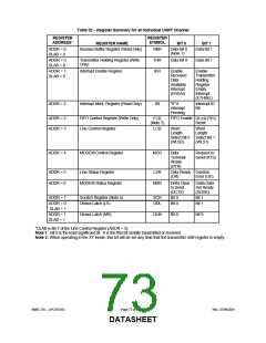
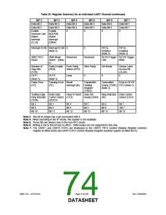
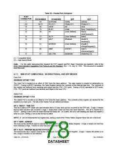
Table 32- Register Summary for an Individual UART Channel (continued)
BIT 2
Data Bit 2
Data Bit 2
Enable
BIT 3
Data Bit 3
Data Bit 3
Enable
BIT 4
Data Bit 4
Data Bit 4
0
BIT 5
Data Bit 5
Data Bit 5
0
BIT 6
Data Bit 6
Data Bit 6
0
BIT 7
Data Bit 7
Data Bit 7
0
Receiver Line MODEM
Status
Status
Interrupt
(ELSI)
Interrupt
(EMSI)
Interrupt ID Bit Interrupt ID Bit
(Note 5)
0
0
FIFOs
Enabled
(Note 5)
FIFOs
Enabled
(Note 5)
XMIT FIFO
Reset
DMA Mode
Select (Note
6)
Reserved
Reserved
Stick Parity
0
RCVR Trigger RCVR Trigger
LSB
MSB
Number of
Stop Bits
(STB)
Parity Enable Even Parity
Set Break
Divisor Latch
Access Bit
(DLAB)
(PEN)
Select (EPS)
OUT1
OUT2
Loop
0
0
(Note 3)
(Note 3)
Parity Error
(PE)
Framing Error Break
(FE) Interrupt (BI)
Transmitter
Holding
Register
(THRE)
Transmitter
Empty (TEMT) FIFO (Note 5)
(Note 2)
Error in RCVR
Trailing Edge Delta Data
Clear to Send Data Set
Ring Indicator Data Carrier
Ring Indicator Carrier Detect (CTS)
Ready (DSR) (RI)
Detect (DCD)
(TERI)
(DDCD)
Bit 2
Bit 2
Bit 10
Bit 3
Bit 3
Bit 11
Bit 4
Bit 4
Bit 12
Bit 5
Bit 5
Bit 13
Bit 6
Bit 6
Bit 14
Bit 7
Bit 7
Bit 15
Note 3: This bit no longer has a pin associated with it.
Note 4: When operating in the XT mode, this register is not available.
Note 5: These bits are always zero in the non-FIFO mode.
Note 6: Writing a one to this bit has no effect. DMA modes are not supported in this chip.
Note 7: The UART1 and UART2 FCR’s are shadowed in the UART1 FIFO Control Shadow Register (runtime
register at offset 0x20) and UART2 FIFO Control Shadow Register (runtime register at offset 0x1D).
SMSC DS – LPC47S45x
Page 74 of 259
Rev. 07/09/2001
DATASHEET

 SMSC [ SMSC CORPORATION ]