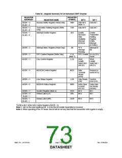
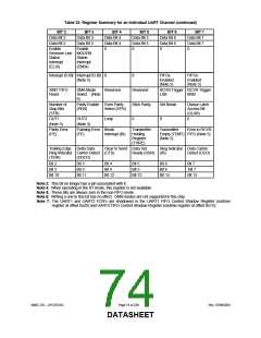
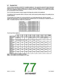
Table 32 − Register Summary for an Individual UART Channel
REGISTER
ADDRESS*
REGISTER
SYMBOL
REGISTER NAME
BIT 0
BIT 1
ADDR = 0
DLAB = 0
ADDR = 0
DLAB = 0
ADDR = 1
DLAB = 0
Receive Buffer Register (Read Only)
RBR
Data Bit 0
(Note 1)
Data Bit 1
Transmitter Holding Register (Write
Only)
THR
IER
Data Bit 0
Data Bit 1
Interrupt Enable Register
Enable
Received
Data
Enable
Transmitter
Holding
Available
Interrupt
(ERDAI)
Register
Empty
Interrupt
(ETHREI)
ADDR = 2
Interrupt Ident. Register (Read Only)
IIR
"0" if
Interrupt
Pending
Interrupt ID
Bit
ADDR = 2
ADDR = 3
FIFO Control Register (Write Only)
Line Control Register
FCR
(Note 7)
FIFO Enable RCVR FIFO
Reset
LCR
Word
Word
Length
Length
Select Bit 0 Select Bit 1
(WLS0)
(WLS1)
ADDR = 4
MODEM Control Register
MCR
Data
Request to
Send (RTS)
Terminal
Ready
(DTR)
ADDR = 5
ADDR = 6
Line Status Register
LSR
Data Ready Overrun
(DR)
Error (OE)
MODEM Status Register
MSR
Delta Clear
to Send
(DCTS)
Delta Data
Set Ready
(DDSR)
ADDR = 7
ADDR = 0
DLAB = 1
ADDR = 1
DLAB = 1
Scratch Register (Note 4)
Divisor Latch (LS)
SCR
DDL
Bit 0
Bit 0
Bit 1
Bit 1
Divisor Latch (MS)
DLM
Bit 8
Bit 9
*DLAB is Bit 7 of the Line Control Register (ADDR = 3).
Note 1: Bit 0 is the least significant bit. It is the first bit serially transmitted or received.
Note 2: When operating in the XT mode, this bit will be set any time that the transmitter shift register is empty.
SMSC DS – LPC47S45x
Page 73 of 259
Rev. 07/09/2001
DATASHEET

 SMSC [ SMSC CORPORATION ]