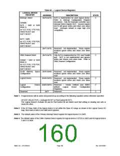
SMSC Defined Logical Device Configuration Registers
The SMSC Specific Logical Device Configuration Registers reset to their default values only on hard resets
generated by Vcc or VTR POR (as shown) or the PCI_RESET# signal. These registers are not affected by soft
resets.
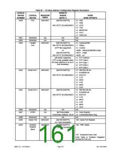
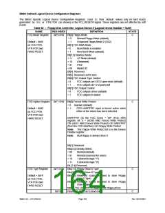
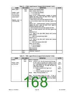
Table 68 – Floppy Disk Controller, Logical Device 0 [Logical Device Number = 0x00]
NAME
FDD Mode Register
REG INDEX
0xF0 R/W Bit[0] Floppy Mode
DEFINITION
STATE
C
= 0
= 1
Normal Floppy Mode (default)
Enhanced Floppy Mode 2 (OS2)
Default = 0x0E
on VCC POR,
VTR POR and
HARD RESET
Bit[1] FDC DMA Mode
= 0
= 1
Burst Mode is enabled
Non-Burst Mode (default)
Bit[3:2] Interface Mode
= 11
= 10
= 01
= 00
AT Mode (default)
(Reserved)
PS/2
Model 30
Bit[4] Reserved
Bit[5] Reserved, set to zero
Bit[6] FDC Output Type Control
= 0
= 1
FDC outputs are OD12 open drain (default)
FDC outputs are O12 push-pull
Bit[7] FDC Output Control
= 0
= 1
FDC outputs active (default)
FDC outputs tri-stated
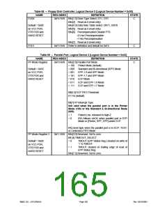
FDD Option Register
0xF1 R/W Bit[0] Forced Write Protect
= 0 Inactive (default)
C
Default = 0x00
on VCC POR,
VTR POR and
HARD RESET
= 1
FDD nWRTPRT input is forced active when
either of the drives has been selected.
nWRTPRT (to the FDC Core) = WP (FDC SRA
register, bit 1) = (nDS0 AND Forced Write Protect)
OR (nDS1 AND Forced Write Protect) OR nWRTPRT
(from the FDD Interface) OR Floppy Write Protect
Note: The Floppy Write Protect bit is in the Device
Disable register.
Note: Boot floppy is always drive 0.
Bit[1] Reserved
Bits[3:2] Density Select
= 00
= 01
= 10
= 11
Normal (default)
Normal (reserved for users)
1 (forced to logic "1")
0 (forced to logic "0")
Bit [7:4] Reserved.
0xF2 R/W Bits[1:0] Floppy Drive A Type
Bits[3:2] Floppy Drive B Type
FDD Type Register
C
C
Default = 0xFF
on VCC POR,
VTR POR and
HARD RESET
Bits[5:4] Reserved (could be used to store Floppy
Drive C type)
Bits[7:6] Reserved (could be used to store Floppy
Drive D type)
Note: The LPC47M14x supports two floppy drives
Reserved, Read as 0 (read only)
0xF3 R
SMSC DS – LPC47M14X
Page 164
Rev. 03/19/2001

 SMSC [ SMSC CORPORATION ]