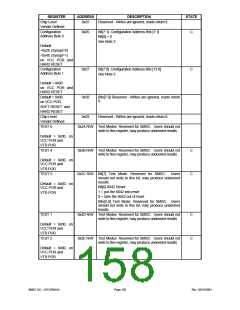
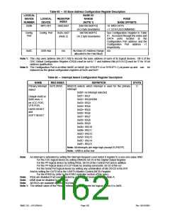
Table 65 – I/O Base Address Configuration Register Description
BASE I/O
LOGICAL
DEVICE
NUMBER
0x0B
LOGICAL
REGISTER
RANGE
FIXED
INDEX
DEVICE
(NOTE 1)
BASE OFFSETS
MPU-401
0x60,0x61
[0x0100:0x0FFE]
on 2-byte boundaries
0x0100:0x0FFE
On 2 byte boundaries
+0: MIDI DATA
+1: STATUS/COMMAND
Config.
Port
Config. Port
USB Hub
0x26, 0x27
(Note 2)
See Configuration Register in Table
61. Accessed through the index and
DATA ports located at the
Configuration Port address and the
Configuration Port address +1
respectively.
0x0C
n/a
No Base I/O Address Range n/a
allocated to the Hub Block
Note 1: This chip uses address bits [A11:A0] to decode the base address of each of its logical devices. Bit 6 of the
OSC Global Configuration Register (CR24) must be set to ‘1’ and Address Bits [A15:A12] must be ‘0’ for 16 bit
address qualification.
Note 2: The Configuration Port is at either 0x02E or 0x04E (for SYSOPT=0 or SYSOPT=1) at power up and can be
replaced via the global configuration registers at 0x26 and 0x27.
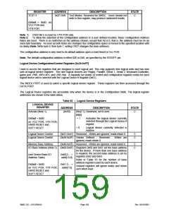
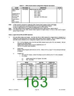
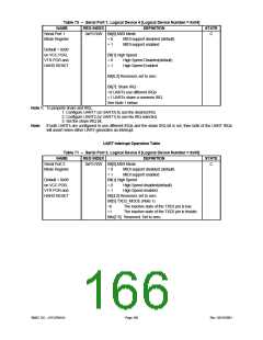
Table 66 – Interrupt Select Configuration Register Description
NAME
REG INDEX
DEFINITION
STATE
Primary Interrupt 0x70 (R/W)
Select
Bits[3:0] selects which interrupt is used for the primary
C
Interrupt.
0x00= no interrupt selected
0x01= IRQ1
0x02= IRQ2/nSMI
0x03= IRQ3
Default=0x00 or
0x06 (Note 1)
on VCC POR,
VTR POR,
0x04= IRQ4
HARD RESET
and
0x05= IRQ5
0x06= IRQ6
SOFT RESET
0x07= IRQ7
0x08= IRQ8
0x09= IRQ9
0x0A= IRQ10
0x0B= IRQ11
0x0C= IRQ12
0x0D= IRQ13
0x0E= IRQ14
0x0F= IRQ15
Note: All interrupts are edge high (except ECP/EPP)
Note: nSMI is active low
Note:
An Interrupt is activated by setting the Interrupt Request Level Select 0 register to a non-zero value AND :
For the FDC logical device by setting DMAEN, bit D3 of the Digital Output Register.
For the PP logical device by setting IRQE, bit D4 of the Control Port and in addition
For the PP logical device in ECP mode by clearing serviceIntr, bit D2 of the ecr.
For the Serial Port logical device by setting any combination of bits D0-D3 in the IER
And by setting the OUT2 bit in the UART's Modem Control (MCR) Register.
For the KYBD by (refer to the KYBD controller section of this spec).
Note: IRQs are disabled if not used/selected by any Logical Device. Refer to Note A.
Note: nSMI must be disabled to use IRQ2.
Note: All IRQ’s are available in Serial IRQ mode.
Note 1: The default value of the Primary Interrupt Select register for logical device 0 is 0x06.
SMSC DS – LPC47M14X
Page 162
Rev. 03/19/2001

 SMSC [ SMSC CORPORATION ]